![]()
![]()
RT-012 - Remodel of the Oktava MK-012 PCB |
This page is very long.
|
|
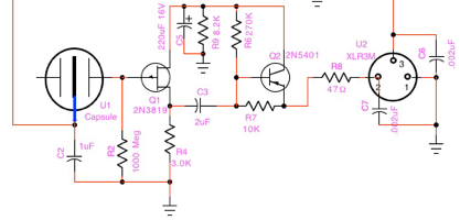
The RT-012 is a pcb which can be used to repair the Oktava MK-012 microphones. The original Russian pcb was not of high quality and many have failed or become unreliable after repairs and modifications. It can also be used to build similar microphones, using either conventional or electret capsules, but please see RT-012-A. The pcb can be used to build a near exact copy of the original circuit, and many of the original components can be simply transferred if they are in good condition. There are some minor differences in the pcb design to enable the use of radial-leaded easy to get high quality electrolytic capacitors. Also in the schematic I have suggested some component value changes to slightly improve the impedance-balancing of the output and to specify the components as relatively easy to get "normal" values. Another aim of the design is to provide a higher quality double sided pcb that can take a bit of experimenting with, as people are so fond of doing. If you are careful with it, it will stand for components being changed without falling apart as easily as the original ones do. |
|

|
|

|
MK-012 with original pcb damaged by repairs and mods |
 |
MK-012 with new RT-012 board fitted |

|
Capacitor mounted on back of pcb similarly to the original design. The 10n ceramic caps can also be mounted here as in the original design if required. |

|
PCB ready for fitting to microphone |

|
This image is a png file. To see full size, right-click>view image, then click on image or ctrl-scroll to adjust size.
|
Fitting the PCBIdeally the board should be a smooth sliding fit in the tube. If it is too loose there is a chance that resonances will spoil the response of the microphone. If there is damage to the tube the board may become so tight that it is difficult to remove. The first thing you need to do is check the fit of the board to the tube, and if necessary VERY CAREFULLY remove small amounts from the long edges with a flat file. Think in terms of a tenth of a millimetre at a time. Remember to fit a 1mm pin at the IN terminal, for the spring wire to be soldered onto. See picture. Note that the capacitor C4 is mounted on the back of the board. If the ceramic capacitors C7 and C8 are to be included they should be attached at the end of the board as in the original. If using the J201 FET which I specified in the schematic, remember the gate is pin 3 of the package so it is rotated on the pcb pattern as in the picture. This applies to many other FETs, check the data sheet if you are not sure. ALSO PLEASE NOTE that many years ago when I first designed this PCB, I had a large stock of J201 which worked perfectly in this circuit, but more recently (2019) I have had a few reports of problems with it. It seems people have been getting them with IDSS too low to work well. In fact they conform more to the values in the datasheet than the ones I had. In addition there seem to be actual Chinese fakes of these, which are very strange indeed. The assembly is a close fit in the tube and very careful work is needed to make sure that components do not interfere with the tube. Initial testing can easily be done by connecting to a preamp with a good accurate P48 supply. If the volts come out nearly as indicated on the schematic it is fairly certain that all is well. If using a FET with characteristics much different from the original, then obviously you may need to adjust its gate potential. The capsule does not need to be connected for this test, and it is a good idea to connect the input terminal to ground. After stuffing and testing, the board should be defluxed and thoroughly cleaned and dried before reassembling the microphone. Remember leakage can occur through contamination on the components themselves, not just over the pcb. Conformal coating is worth considering, depending on your intended conditions of use. |
| Rodrigo Kremer-Verissimo has been kind enough to construct an LTSpice model of the circuit. | |
|---|---|

|
Please click on image to see .asc file. |
| A customer had some problems with one of these boards and was kind enough to send me the microphone for a closer look. I found that Q2 was faulty and wrongly inserted and the fixing holes at the end of the board near the XLR connector needed to be made slightly larger. Here are some photos. | |
|---|---|
 |
As received. Looks OK, soldering a little messy but I've seen worse. |
 |
Components have been placed neatly and accurately. This is one of the first few batches of this board, and is single-sided. |
 |
The design of the back end has changed over the years. |
 |
|
 |
|
 |
|
 |
|
 |
The board is fitted to the connector after widening the holes slightly. I used screws which are slightly longer than the originals to make the job easier. |
 |
The transistor Q2 has been replaced with a BC212B. P48 is switched on and the circuit voltages agree very closely with the schematic. |
 |
A test signal at the input shows that an output of over 10Vp-p is possible before clipping. |
 |
The capsule contact assembly is cleaned and re-attached and the board is defluxed and cleaned. |
 |
The top surface and components are also cleaned just before reassembly. |
 |
A lot of careful jiggling gets it back together. |
|
Click image to go to Henry's page. |

|
HS-SchoctavaMy redrawing of Henry's circuit. Click the image for a pdf version. Click here for a png version. |
Circuit description:A JFET current source (or sink if you must) passes current through a PNP transistor configured as a Vbe multiplier. At the junction of the JFET drain and the BJT collector a capacitor and a resistor are connected in parallel to ground. Dynamically, signals at the source of the JFET are capacitively coupled to the base of the BJT which then operates as a follower. |
Comments:I think about 1mA would be a good choice of current. This would drop the 48V line by 7V(ish), giving us an unloaded output swing of about 14V before clipping. Clipping would be very asymmetrical, but it's not going to happen because the signal at the FET source will not reach that level. The remaining 40V lets us have 20V for each transistor, which is pleasantly symmetrical. I would propose passing about 50 microamps through the two resistors on the PNP base, making R8 15k and R7 180k. Pretty close to Henry's values. C5 would need to be a 35V device. Not sure why we need R4. I think it's better to let the JFET have all the current, might improve its output impedance a bit. |

|
RT-Schoctava:My redrawing with some mods. Click the image for a pdf version. Click here for a png version.
My mods:
Removed the drain to ground resistor.
Advice:Use something better than the 2N5401 for Q2.Maybe 1mA is rather miserly. 2mA would still leave about 30V over the two transistors, and no need for a fat JFET. Worth thinking about. |

|
A PCB design to fit the MXL 991 microphone.
Right-click>view image to embiggen. |

|
A first attempt to get it working.
|

|
Here is the MXL 991 that I am going to put it in. Quite a nice piece of work, these are good value mics. |

|
Fits in with no problems at all. At least I got that right first time. |

|
Ready for some testing and recording, before I mess about with it some more. |

|
Some more messing about. If I stubbornly stick to the J113, I'm not going to get what I want without an extra resistor in the source, so I divided it into two 470 ohm resistors and ended up with this on the back of the PCB. I think the next batch of boards will have this, it does make it much easier to deal with a FET you want to use but isn't playing along. And the mic does sound remarkably good to me, though I have not yet put it to any serious use.
|
|
|
New schematic showing the resistor added to the source circuit, and some voltage and current values. Click image for pdf.
|
I checked out a few other FETs that I had around -
U1898/J111with the tap at 0% gives Vs=4V, which with R4+R9=1k gives a current of 4mA. This is usable maybe with some slight adjustments.J201I don't think this is usable, at least none of the examples I tried would play nice. Forget about it unless you want to totally rethink the circuit. One of my favourite FETs but it just doesn't have enough IDSS2N3819Seems exactly like the J113.VCR2NThis one is interesting. It is a FET marketed as ideal for voltage-controlled resistor applications. With the tap at 0% (ie R9=0) we get a little over 4V at the source. Might try some further experiments with that. |
|
Capacitors
| ||
| MULTICOMP MCPBSFC-1J102KA45 polyester | 1685470 | |
| KEMET R82EC1100Z350J Film Capacitor, 1000 pF, PET (Polyester), 100 V | 1679411 | |
| WIMA FKP2D011001D00HSSD Film Capacitor, PP (Polypropylene) | 1890176 | Also see AMCH film capacitors for C1 http://www.partsconnexion.com/prod_pdf/amch.pdf> |
| 10n | ||
| KEMET C315C103K1R5TA Multilayer Ceramic Capacitor, Gold Max X7R | 1457642 | |
| 100n | ||
| EPCOS B32529C0104K000 PET | 9750878 | |
| WIMA MKS2C031001A00KSSD Film Capacitor, 0.1 µF, PET (Polyester) | 1006030 | |
| VISHAY BFC237021104 Film Capacitor, 0.1 µF, PET (Polyester) | 1215515 | |
| 220n | ||
| KEMET SMR5224J63J03L16.5CBULK PPS | 2529177 | |
| KEMET R82DC3220DQ60J Film Capacitor, 0.22 µF, PET (Polyester) | 2429338 | |
| 1/63 | ||
| MULTICOMP MCGPR63V105M5X11 | 9451455 | |
| KEMET ESK105M063AC3AA | 2069032 | |
| MULTICOMP MCMHR63V105M4X7 | 9452737 | |
| MULTICOMP MCRH63V105M5X11 | 9452001 | |
| 22/63 | ||
| PANASONIC ELECTRONIC COMPONENTS EEUFC1J220 | 9692495 ** | |
| PANASONIC ELECTRONIC COMPONENTS ECA-1JHG220 | 1848558 ** | |
| Resistors | ||
| 1G | ||
| TE Connectivity Manufacturer Part No: RGP0207CHK1G0 | N/A | Mouser Part No: 279-RGP0207CHK1G0
Digikey A106006CT-ND *** |
| Stackpole Electronics Inc. HVA12JA1G00 | N/A | Digikey HVA12JA1G00CT-ND ** |
| OHMITE SM102031007FE | 1550765 | ?? |
| Ohmite Thick Film Resistors 1/4watt 5% MOX-200001007JE | N/A | Mouser Part No: 588-MOX-200001007JE |
| For other resistors I would recommend the TE CONNECTIVITY LR1F series (ie part numbers beginning LR1F). | ||
| FET | ||
| 2N3819 obsolete, old stock available various places,
Farnell suggested equivalent is J112 |
1017712 | |
| J201 ditto PF5102, please see notes about J201 above. | 2454063 | |
| J113 | 1017713 |
end


