![]()
![]()
|
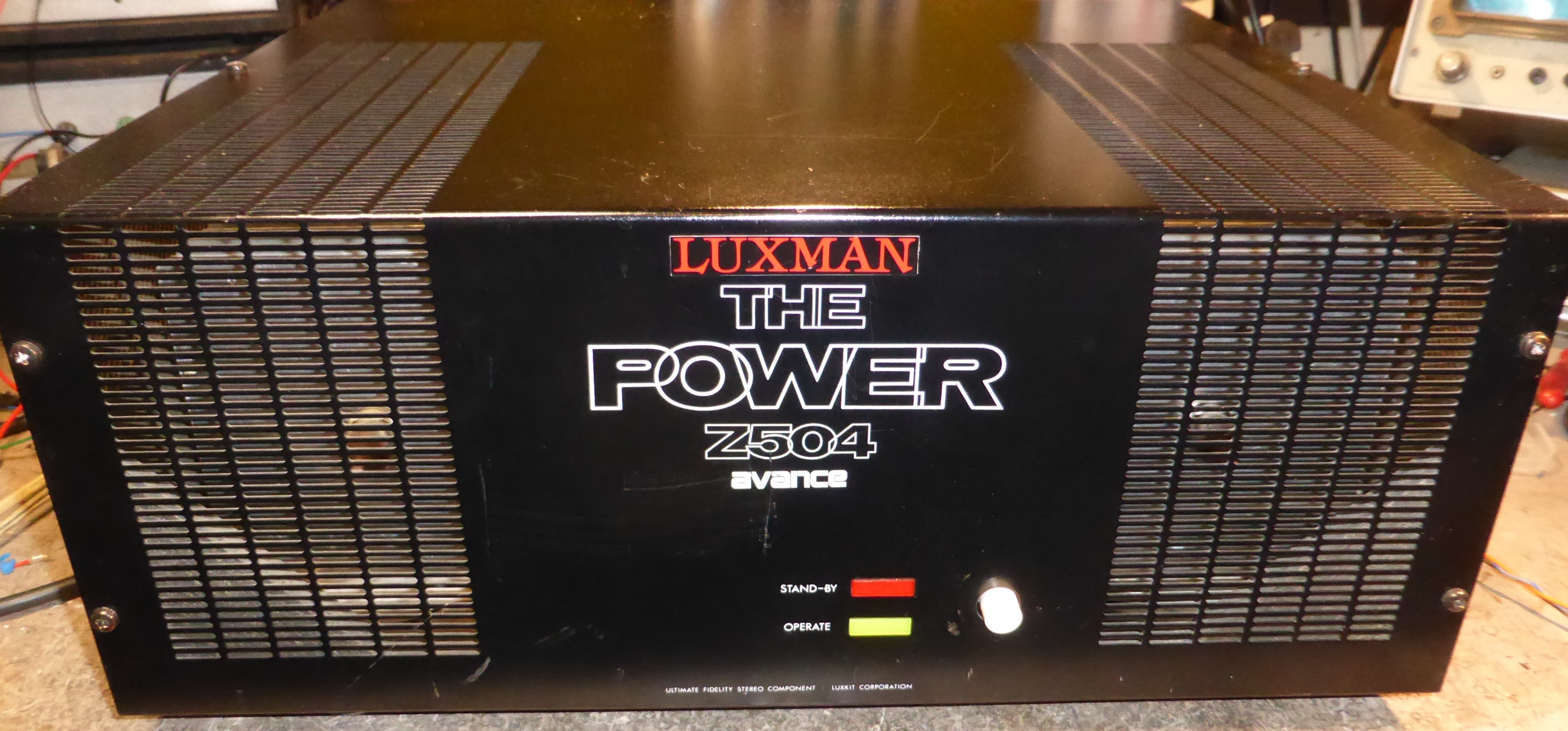
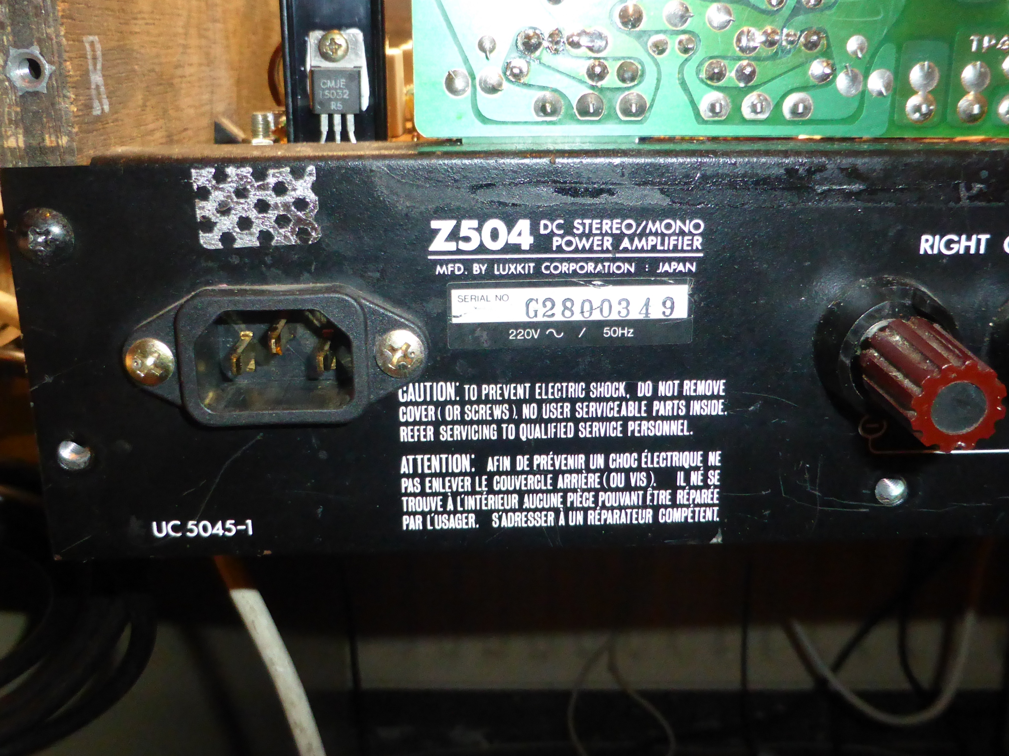
A rare hifi power amp, which was apparently also available as a kit. This one was built by Avance.
|

|
(If you want to embiggen any picture here or on other pages, right-click on it then select view image. Or whatever your browser calls it.)
|
Schematic circuit diagram | |

|
This image is a png file. To see full size, right-click>view image, then click on image or ctrl-scroll to adjust size. Best printed at A3 size, but A4 will work if you have a good printer and eyesight. |
|
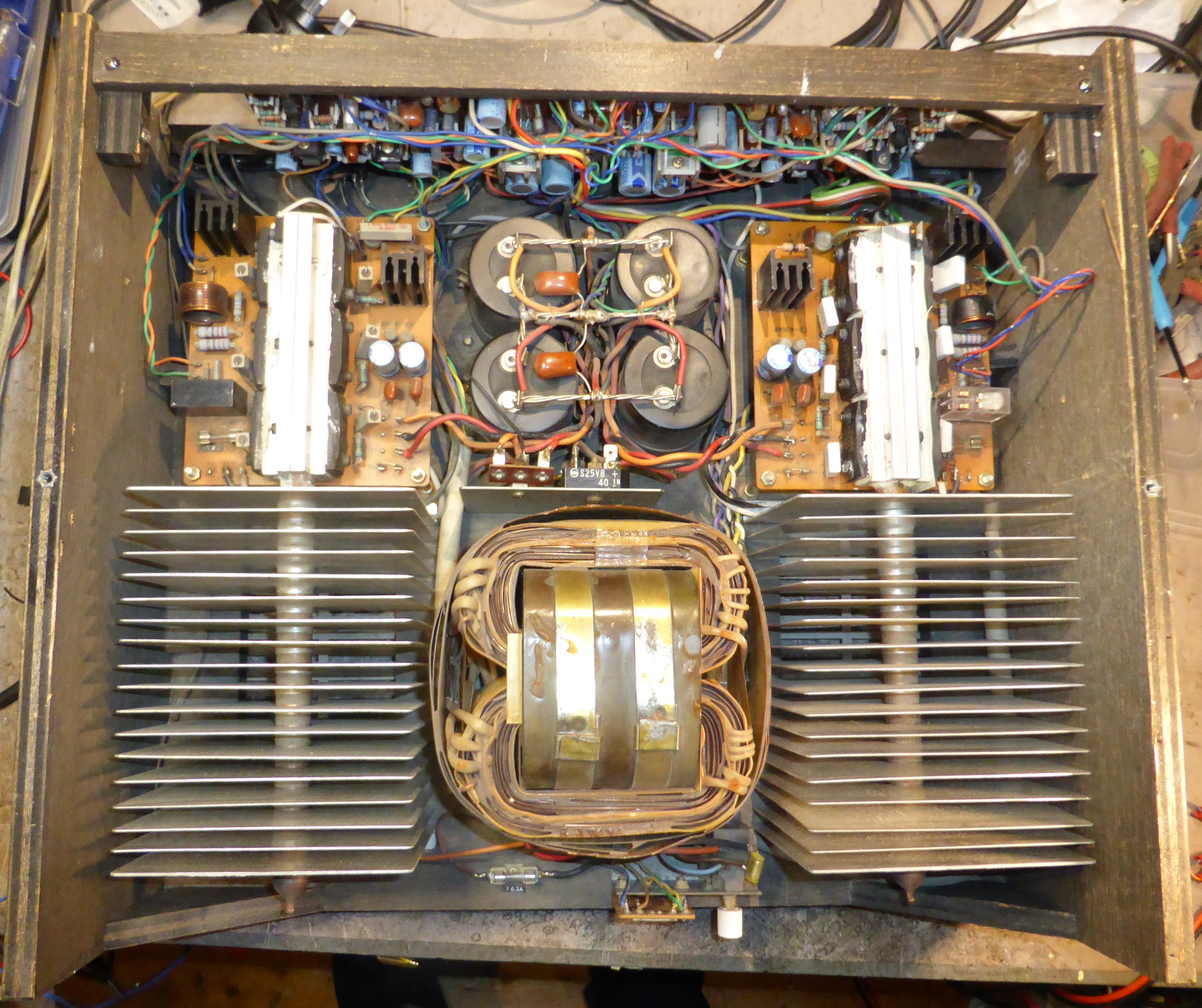
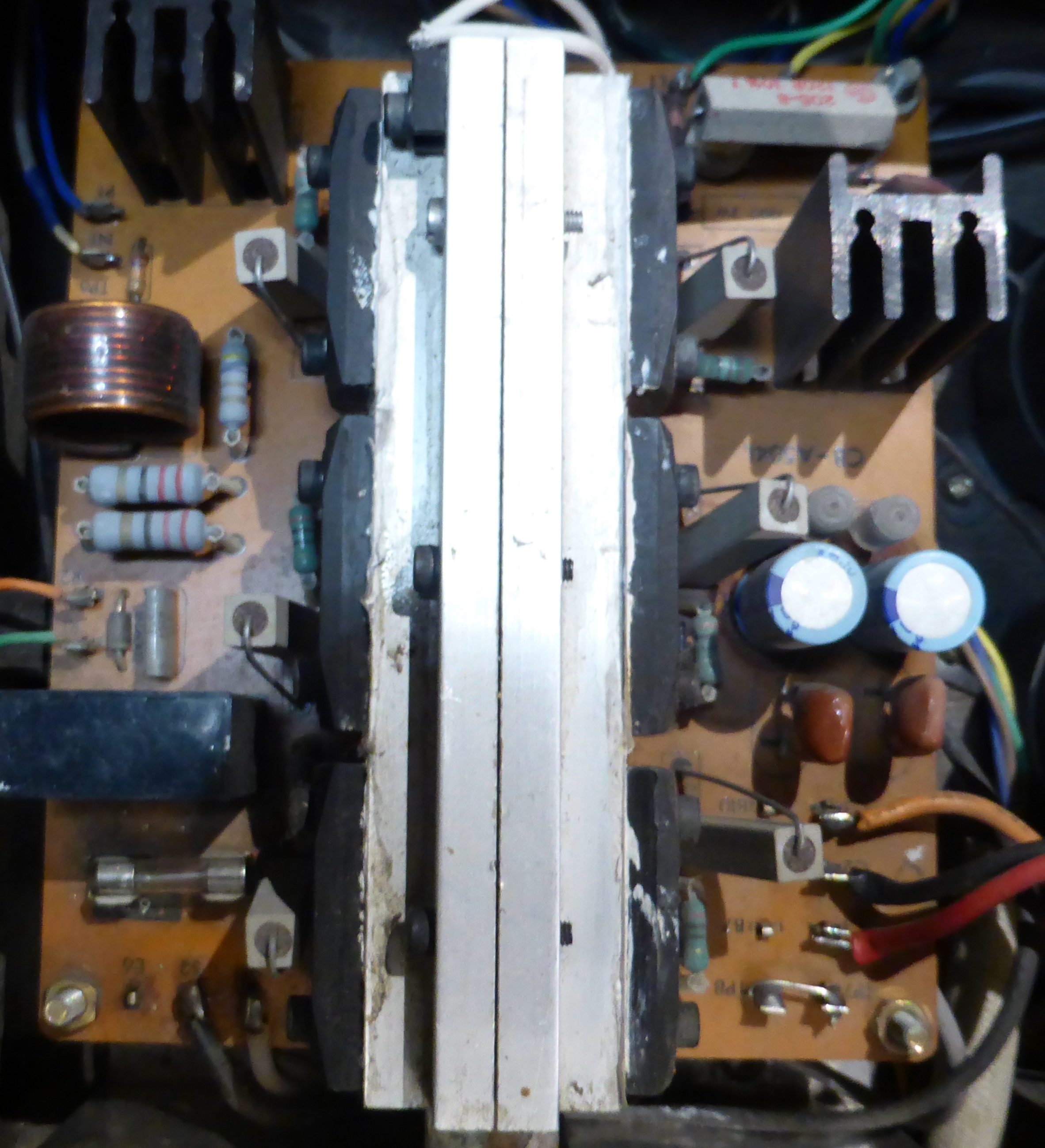
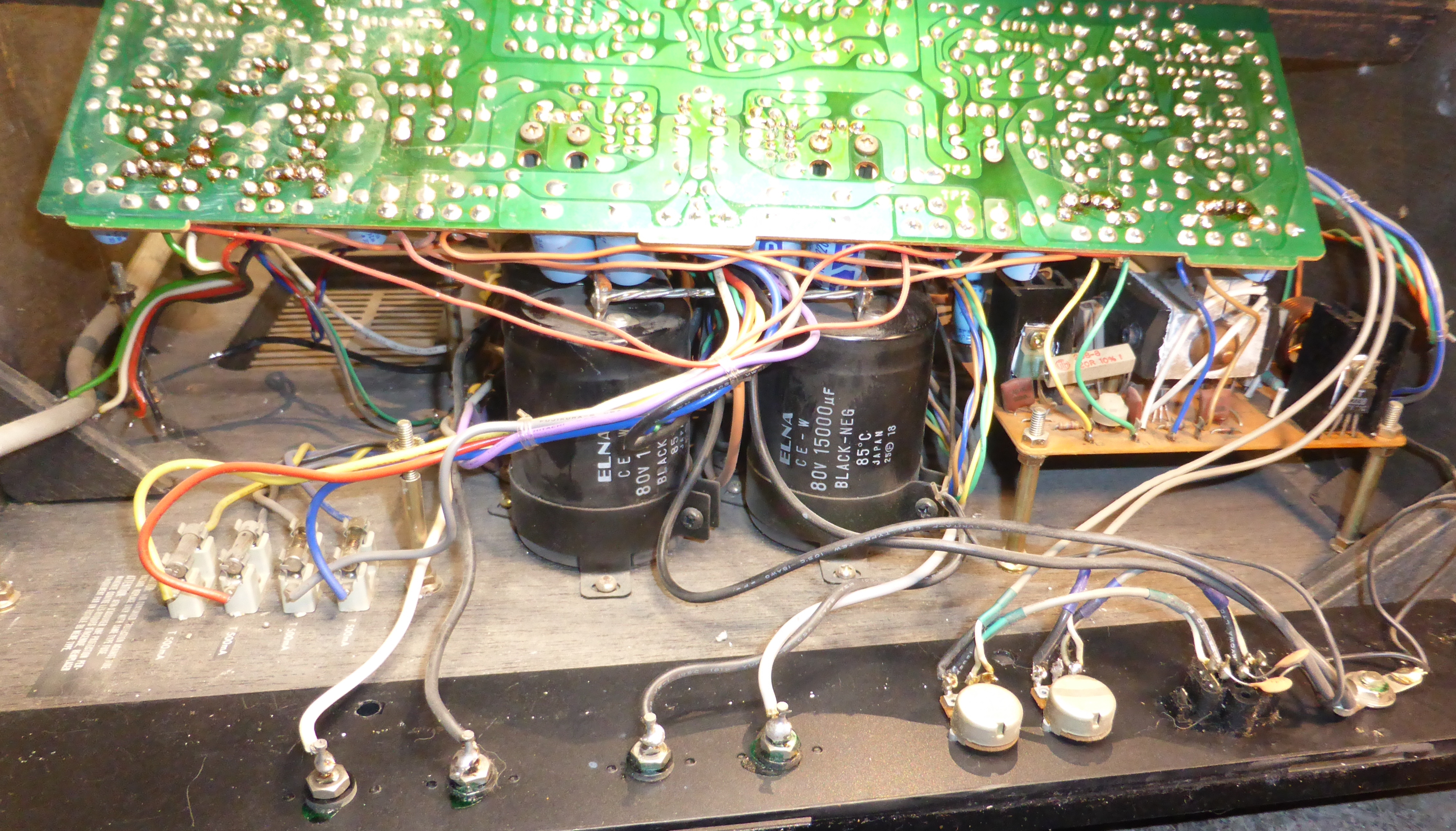
The majority of the circuit is on the back panel PCB. The two PCBs left and right contain the output stages, thermal compensation and a SPNO relay. Much spaghetti. |
|
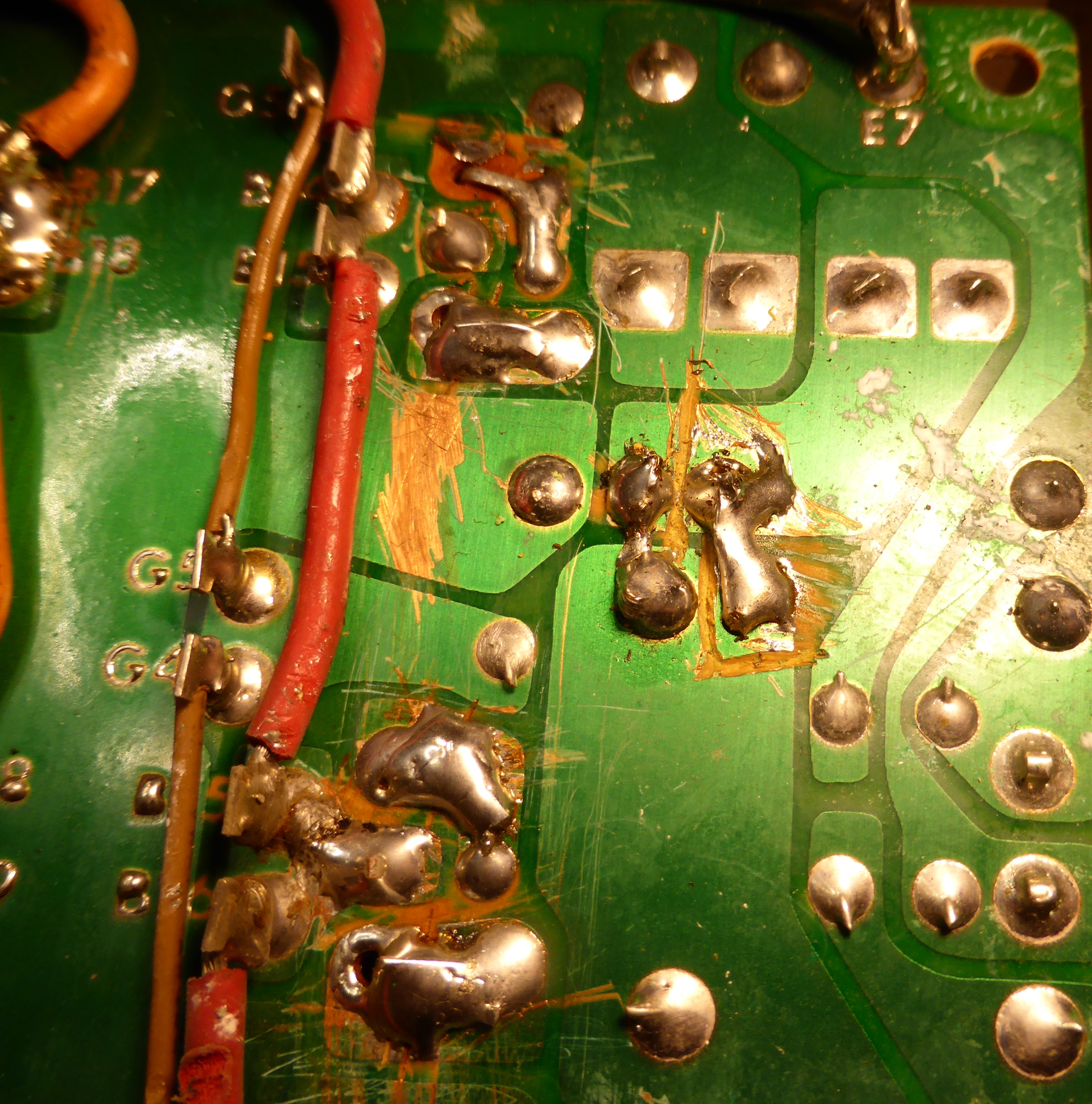
Looking at the most obviously failed (right) channel, it seems we've had the bodgers in. |
|
Now I notice that the relay here seems to have magically transformed into an Omron DPCO. Don't know how that's going to help. |
|
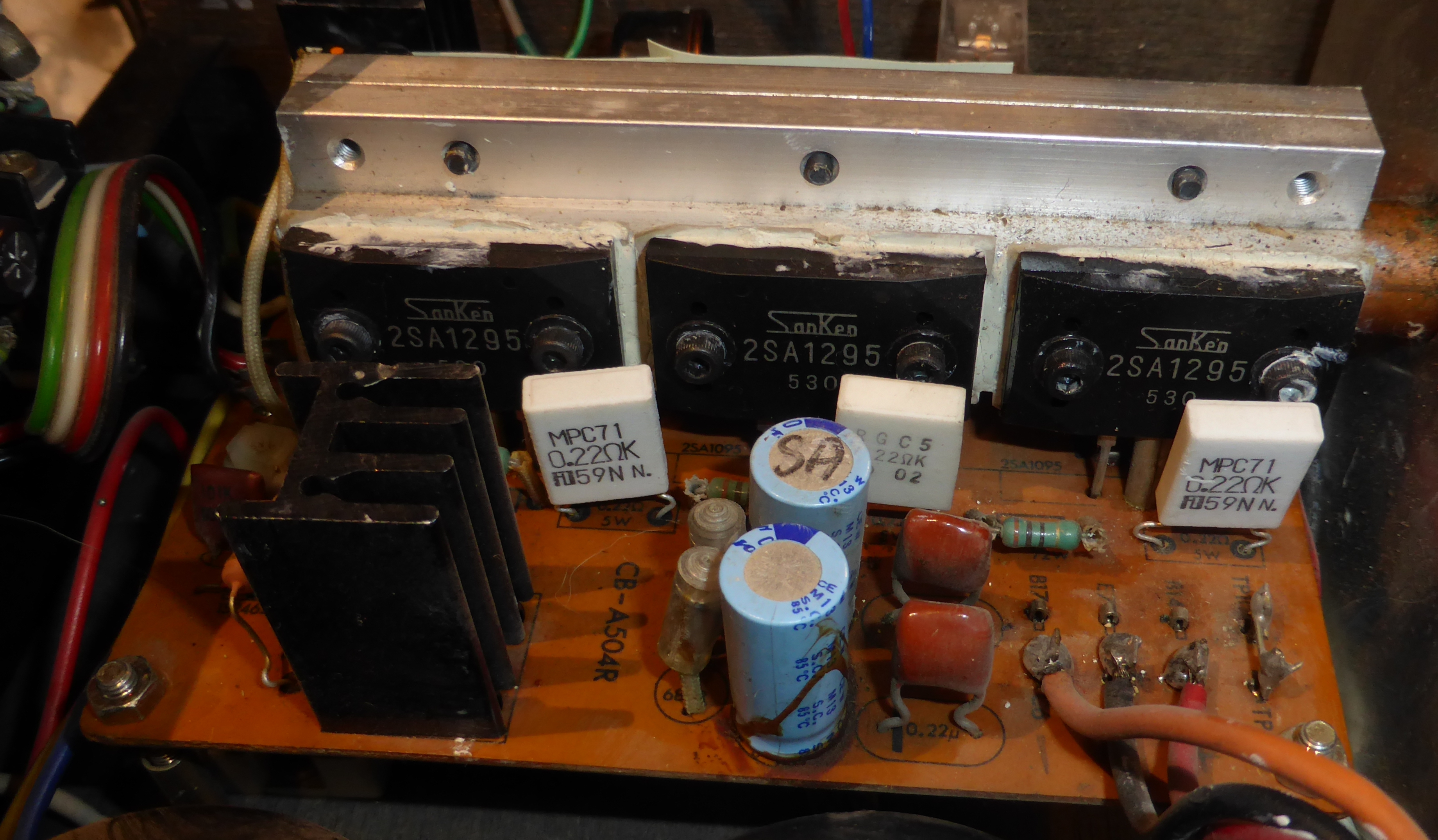
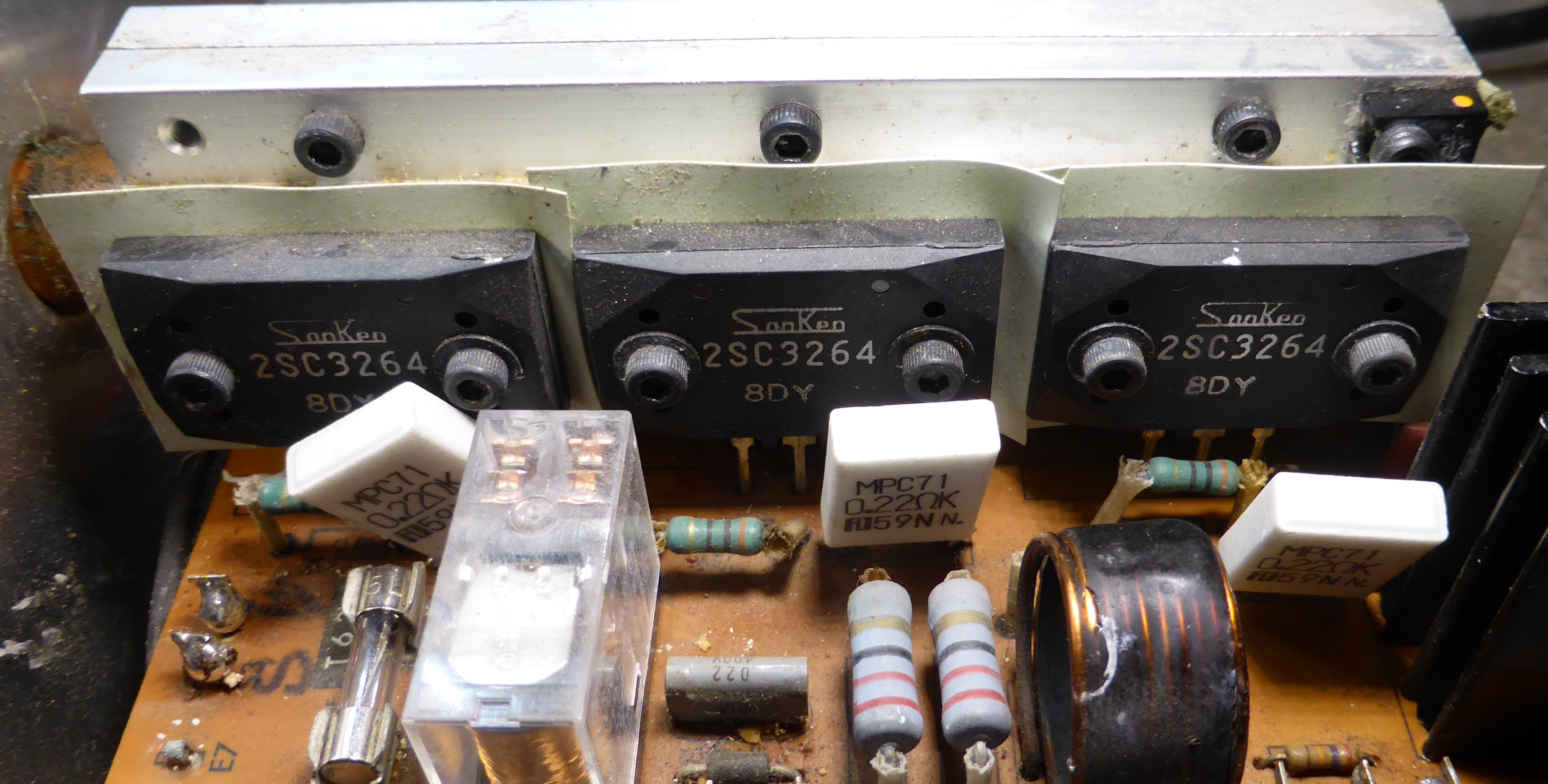
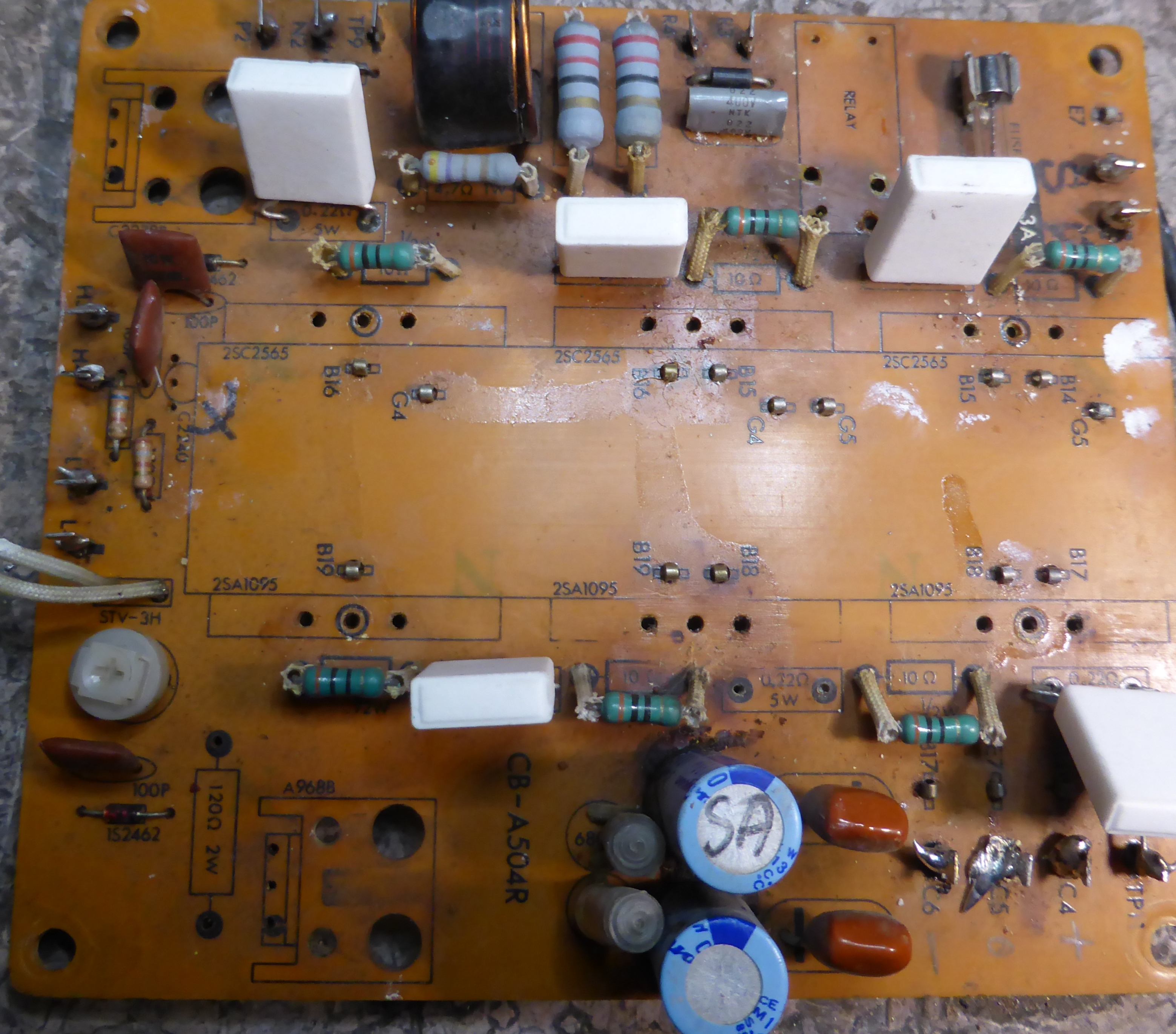
This is the better-looking (left) channel. It looks a lot tidier than the other one, but the 5W resistors don't look right. Could be OK I suppose. Also there is a lot of white gunge on the Sankens. Less is more in my opinion.
|
|
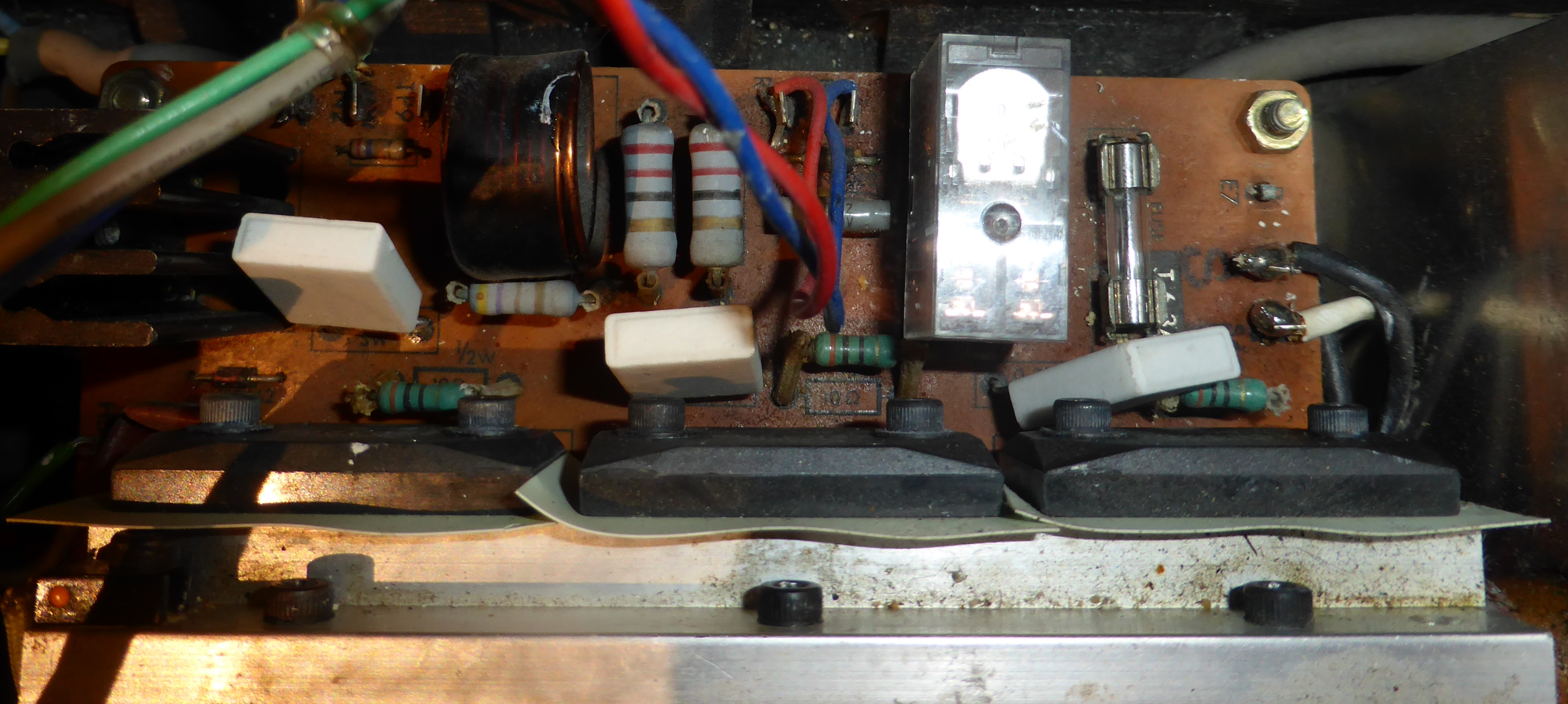
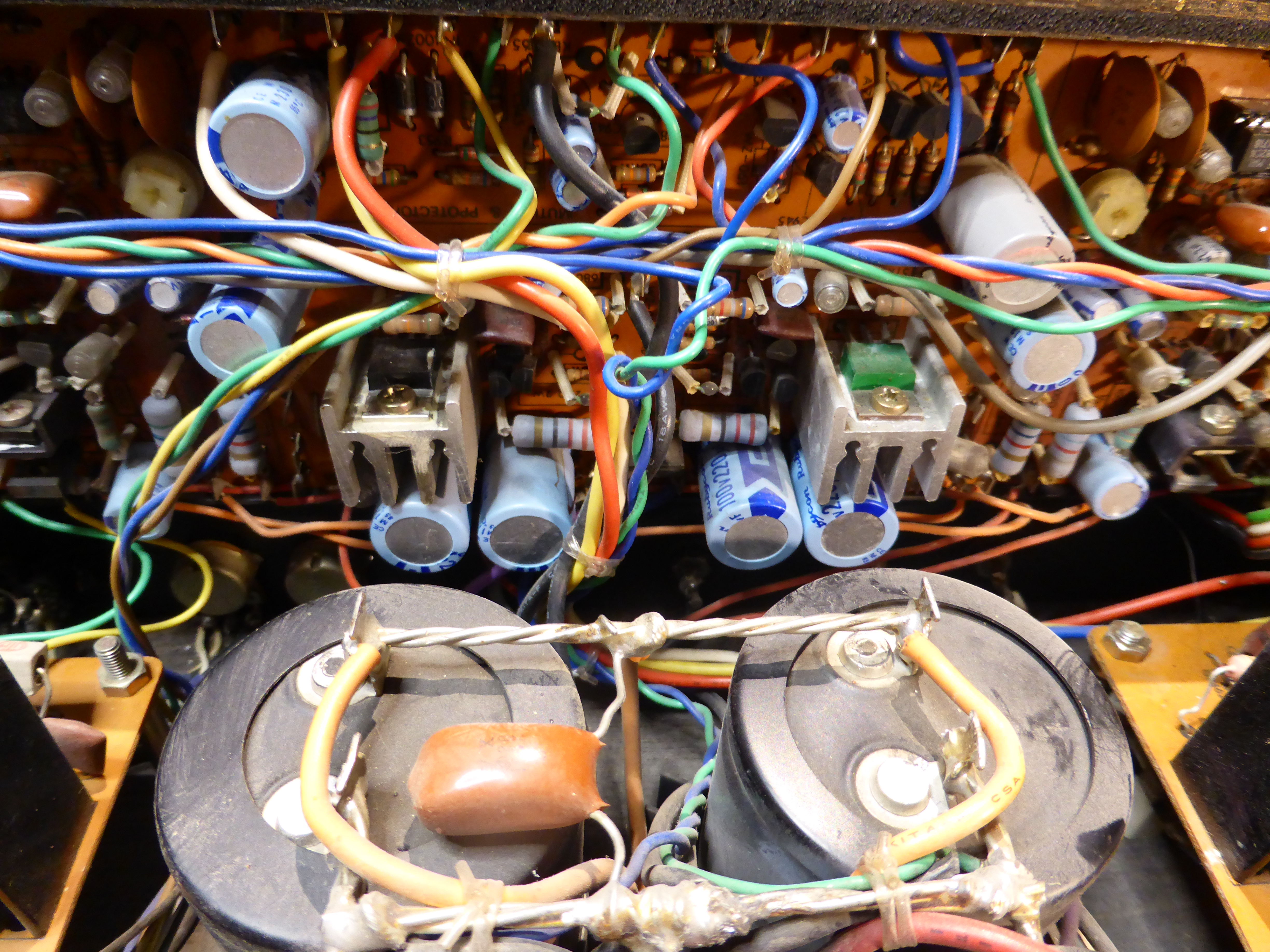
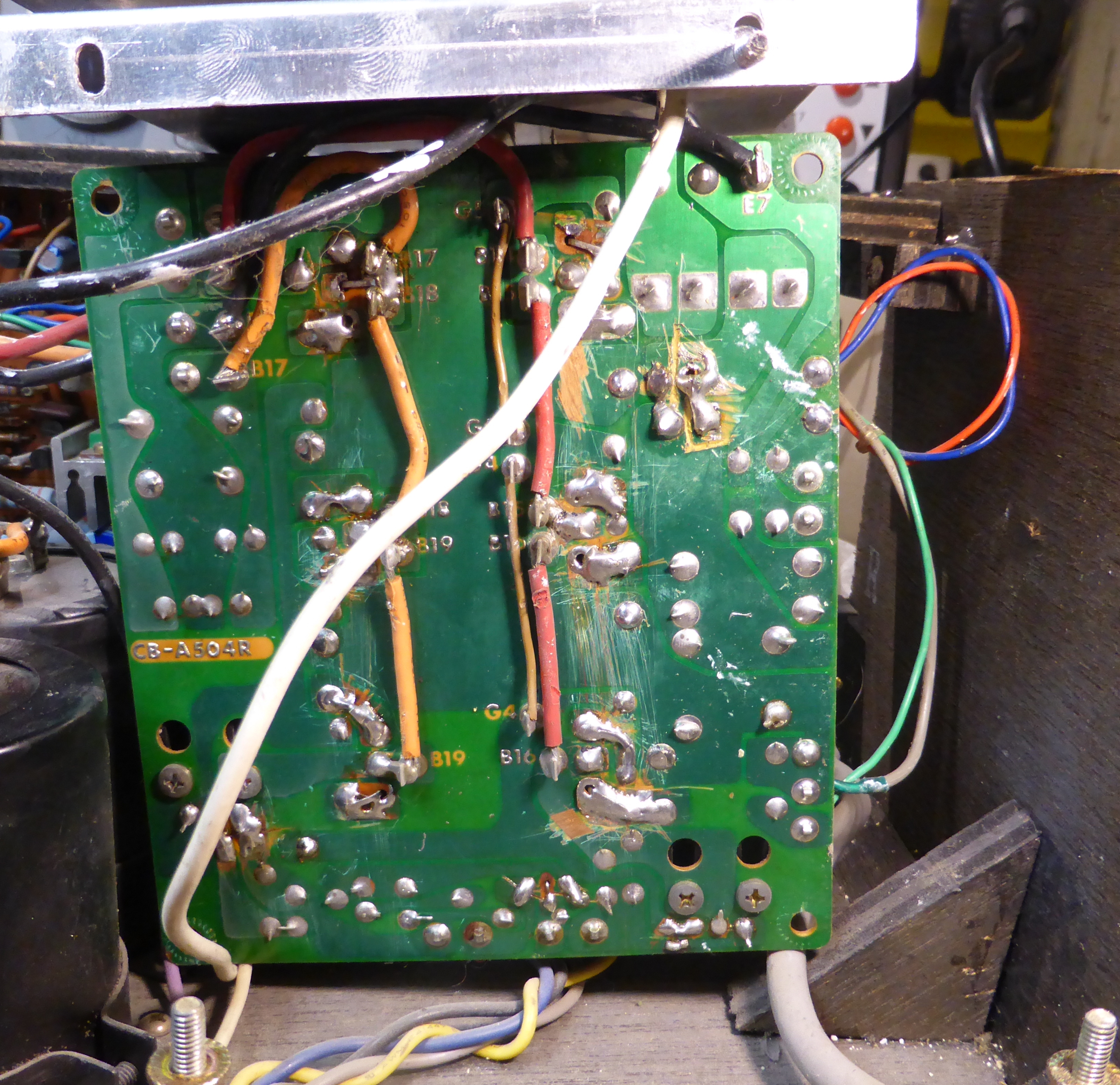
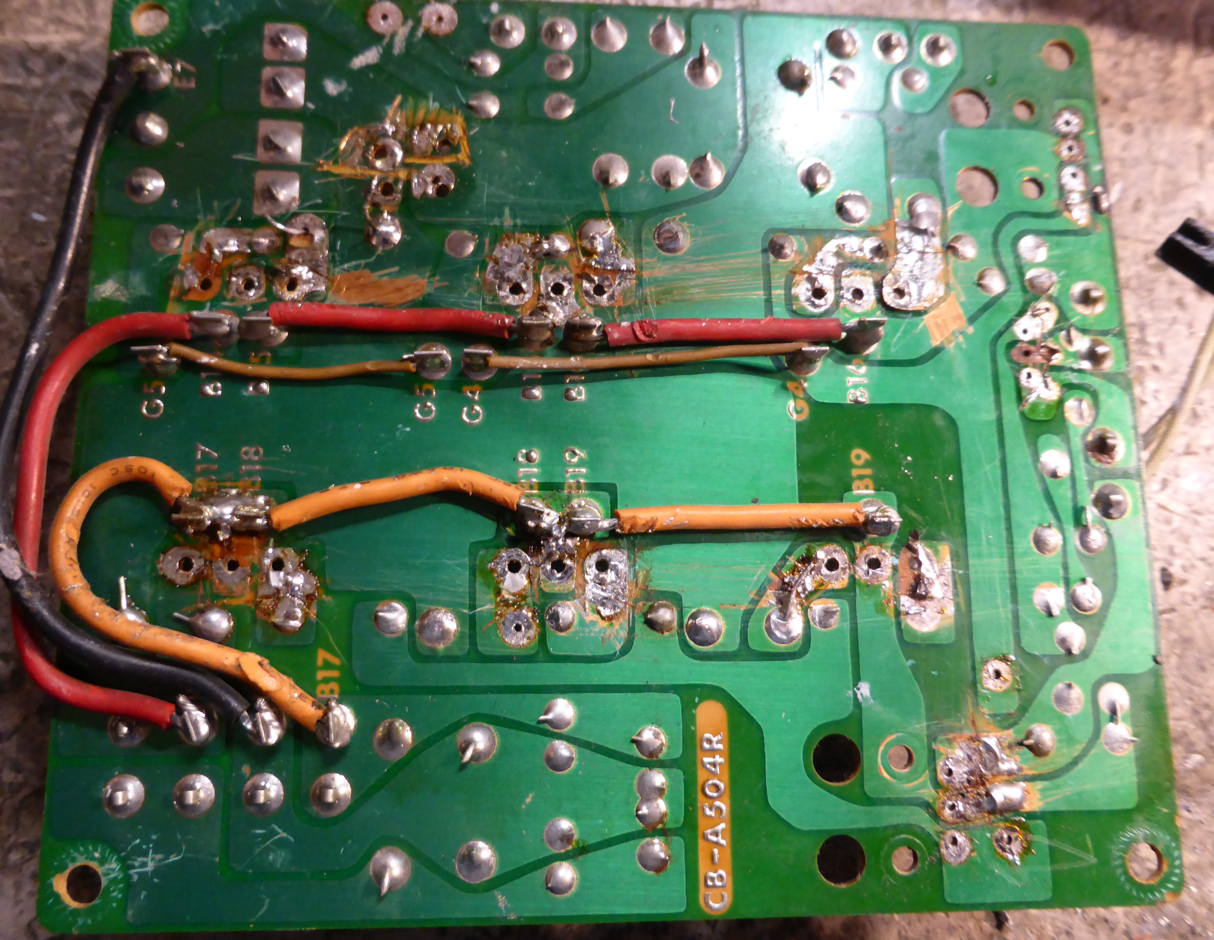
The back PCB. Something soviet has happened here, but I'm not sure what. I will leave it until the output stages are happy. |
|
At the front we have the main power switch and these interesting LED type things. |
|
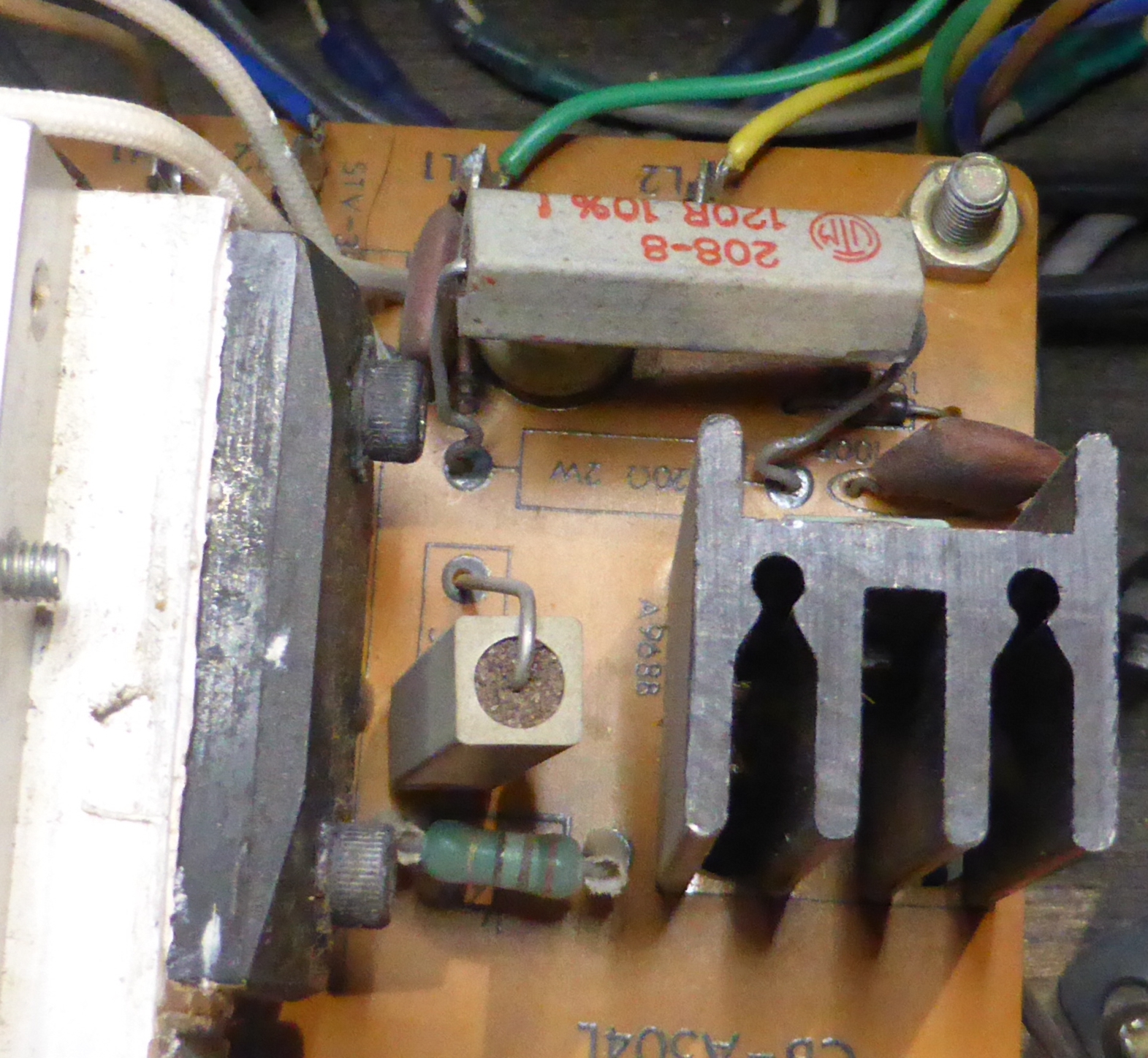
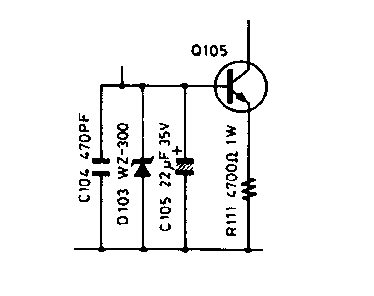
The 120R resistor is burnt, this is an interbasic resistor of the output transistors, so it's fairly certain they are all dead. What you can't see is that one of the wires of the STV-3H thermal diode is broken, which would account for that. |
|
The corresponding resistor on the other channel. |
|
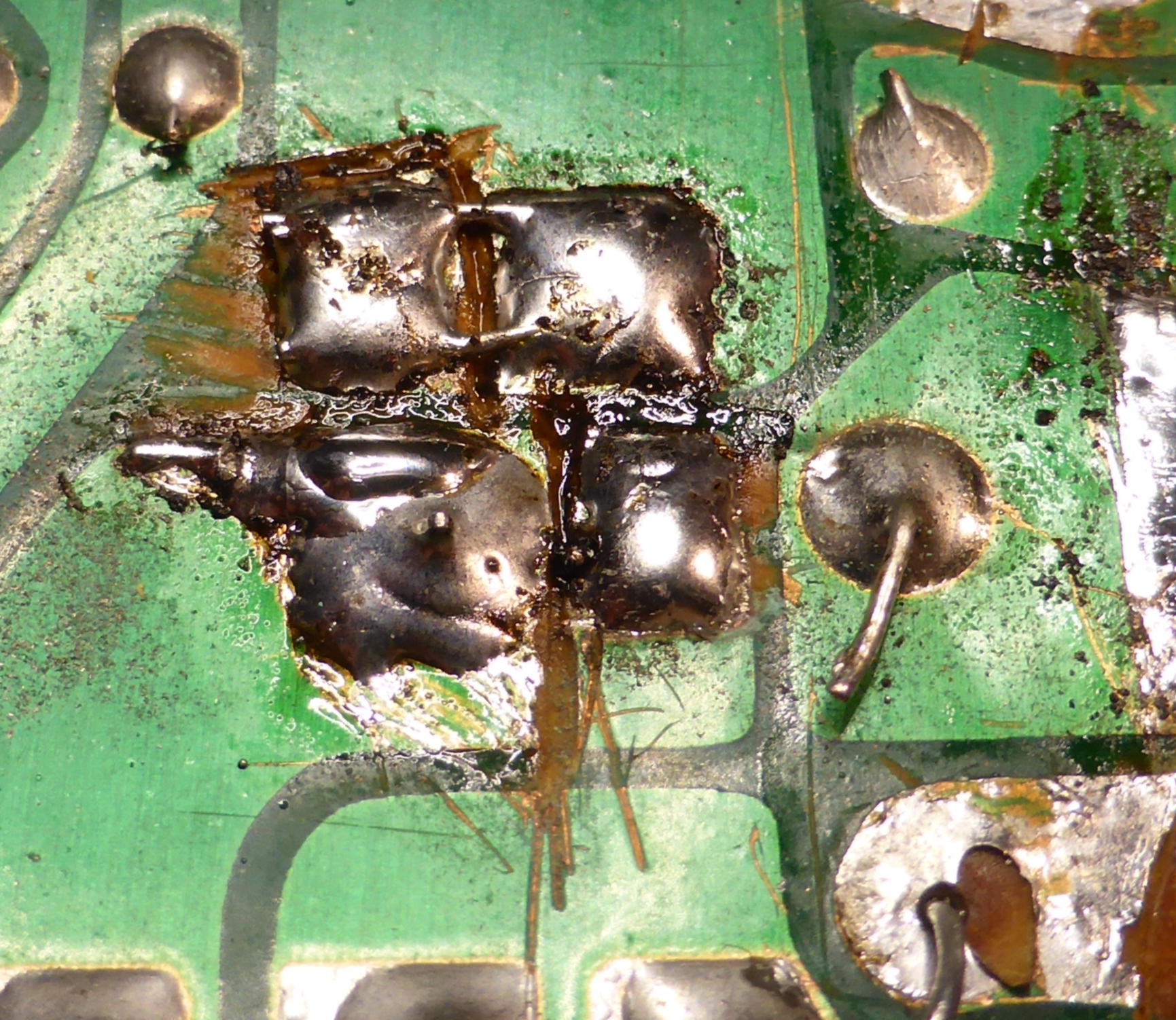
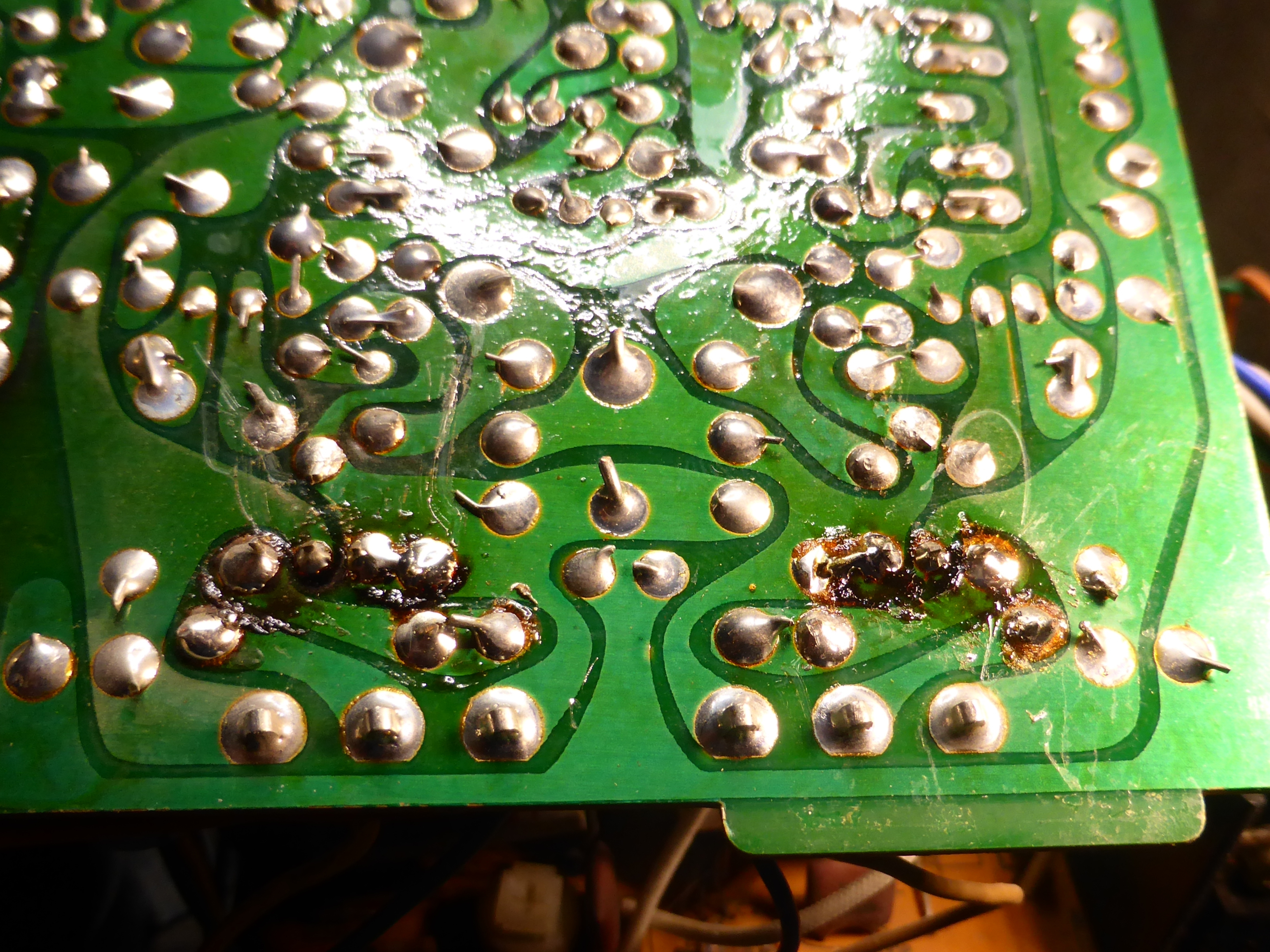
Working on the right channel first, as the left one looks better, I have taken a few screws out to have a look at the tracks. It looks like a bomb has hit it. The solder resist has been scraped off, and many tracks have been hacked through and blobbed with solder. |
|
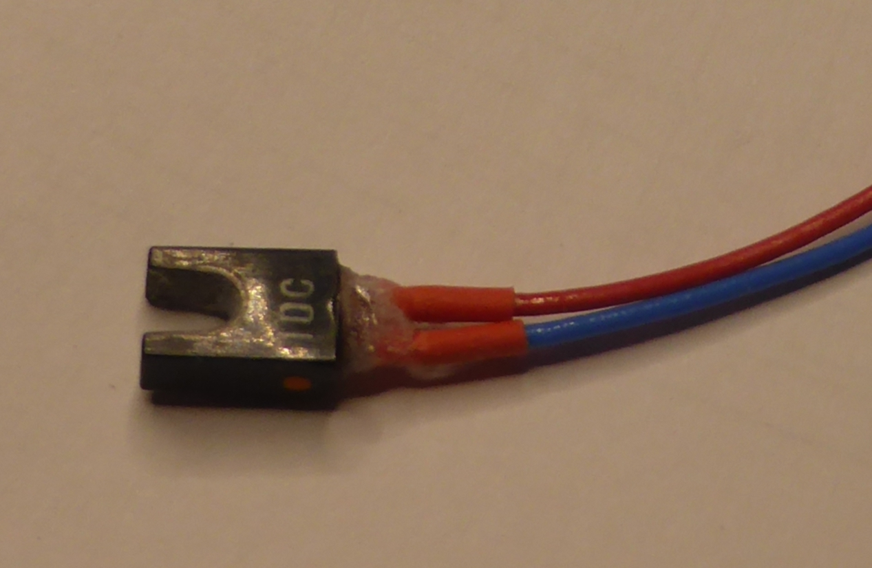
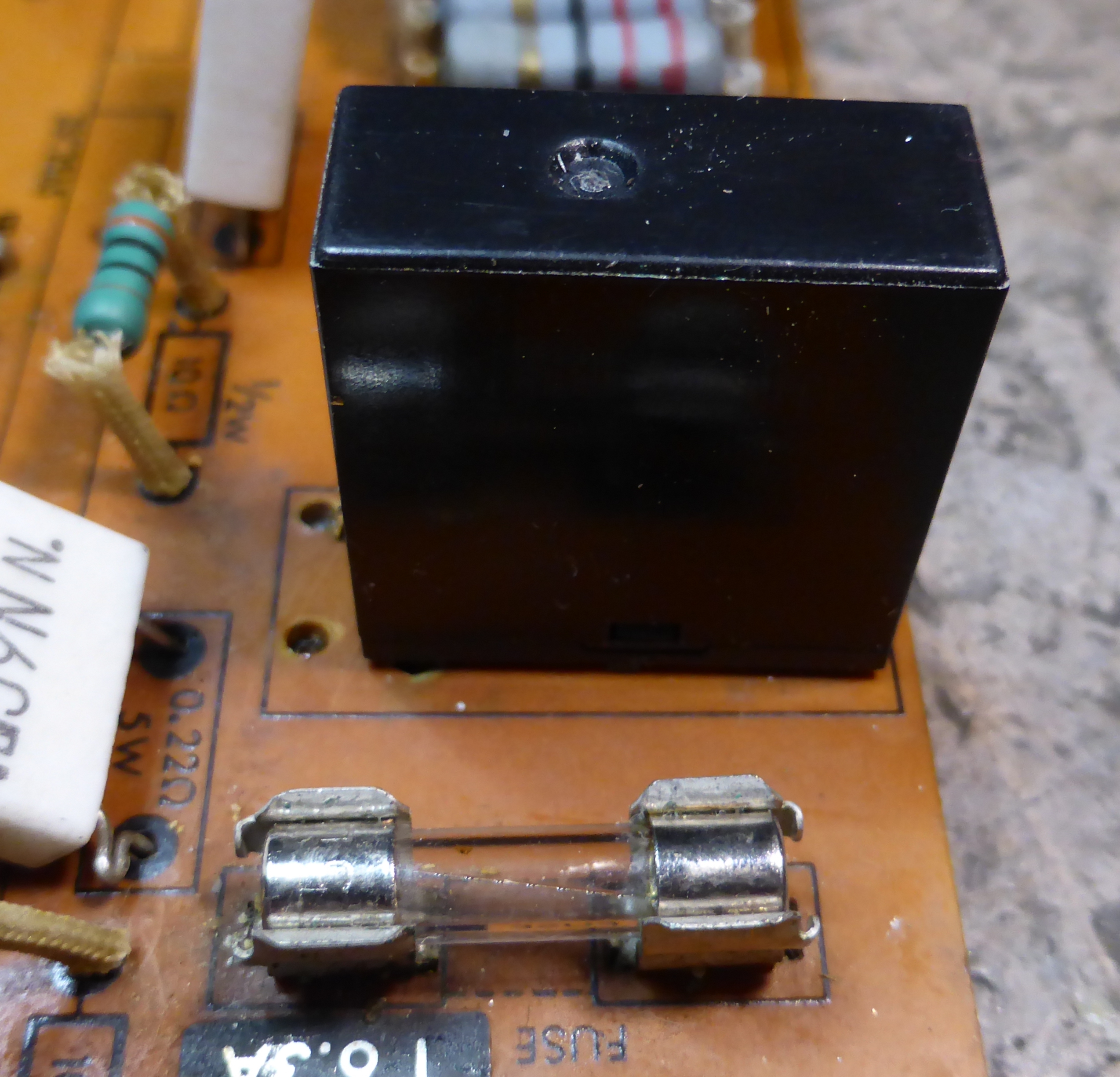
Under the PCB are hidden a few fuses. A strange place to put them. |
|
Note how the mystery wizard of the soldering iron has elected to fit half of the output transistors with the original mica washers, but this side has these elegant pale blue silicone rubber items. |
|
A close-up of some of the modifications. How might this have happened? |
|
Here I have removed all the transistors and the relay. As expected, all nine transistors are dead.
|
|
|
|
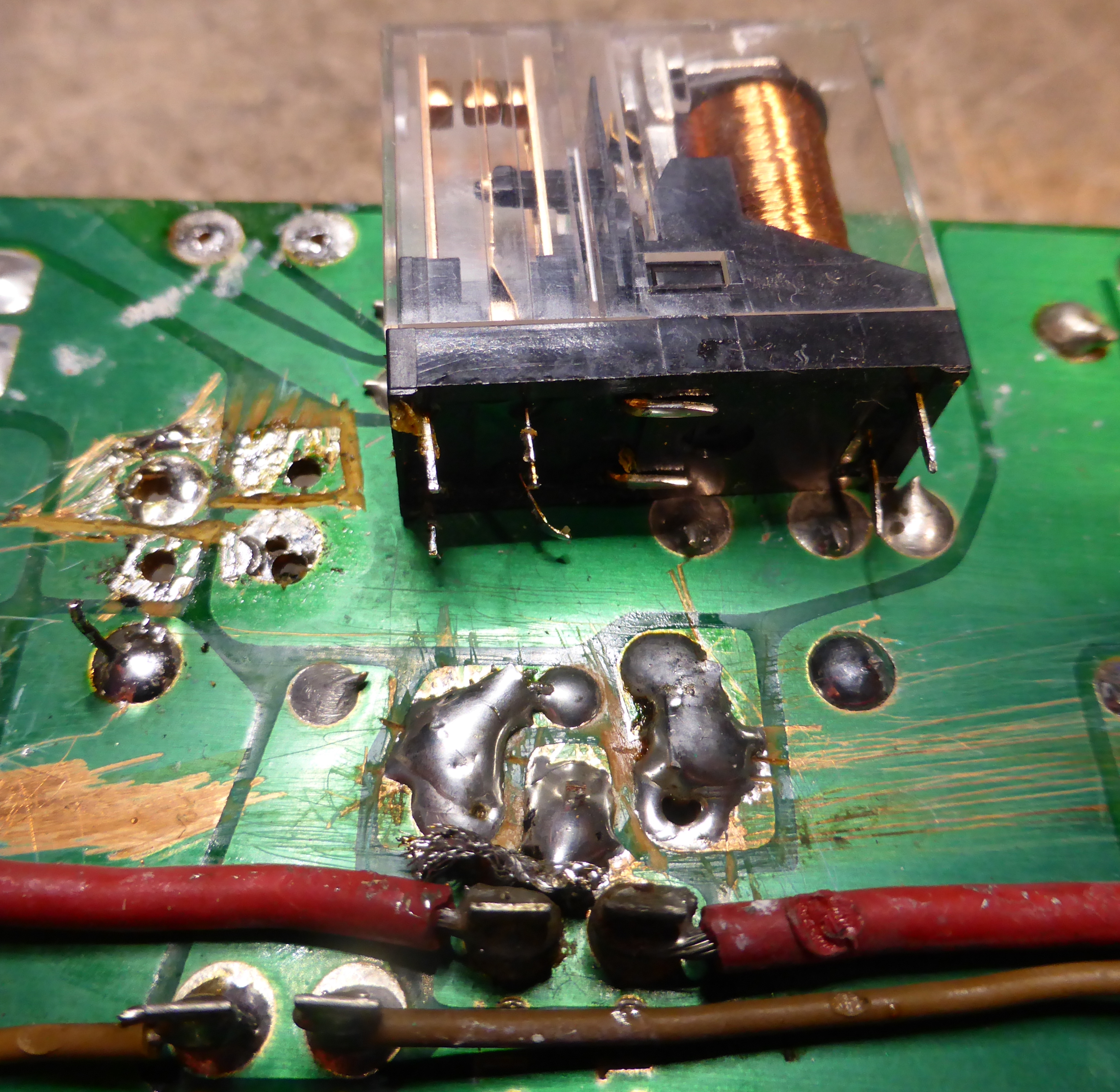
This is how the Omron relay was fitted, the bodging was because this relay works front to back and the original was a left to right type. Also it has eight pins instead of just four. |
|
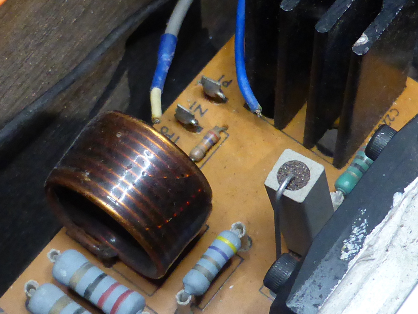
The STV-3H is a device I could not get easily. It is a strange thing which has a forward voltage of around 1.6V, rather less than you would expect from three silicon junctions, and the tempco is also a little less than typical small diodes. What I have done here is excavate the works from the case and glue in a couple of diodes. I have done this before and it worked well. Remains to be seen how well it works here, might have to rethink it. I will also replace the accompanying 2SC2240 with a BC182L, as that has a slightly higher tempco than the holy scriptures would lead you to believe. |
|
Something fairly close to the original relay. This is a TE SDT-S-112DMR. |
|
Bridging some of the disconnected copper. It's going to look lovely when it's finished. |
|
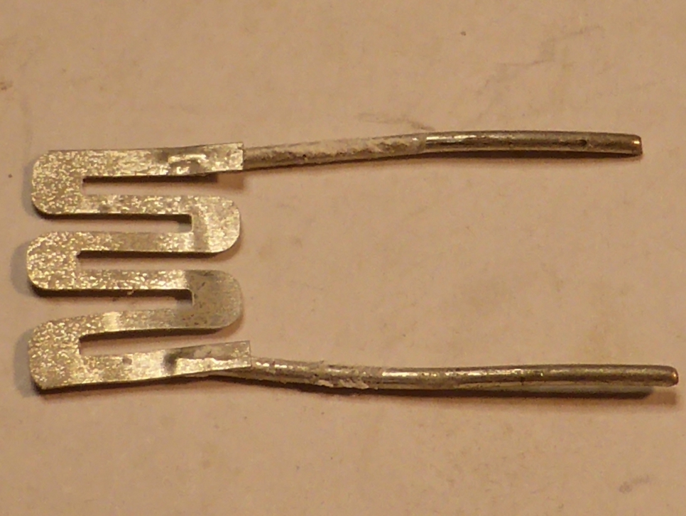
I was suspicious of the new emitter resistors, from a Chinese supplier, so I smashed one open for a look. Not bad at all. |
|
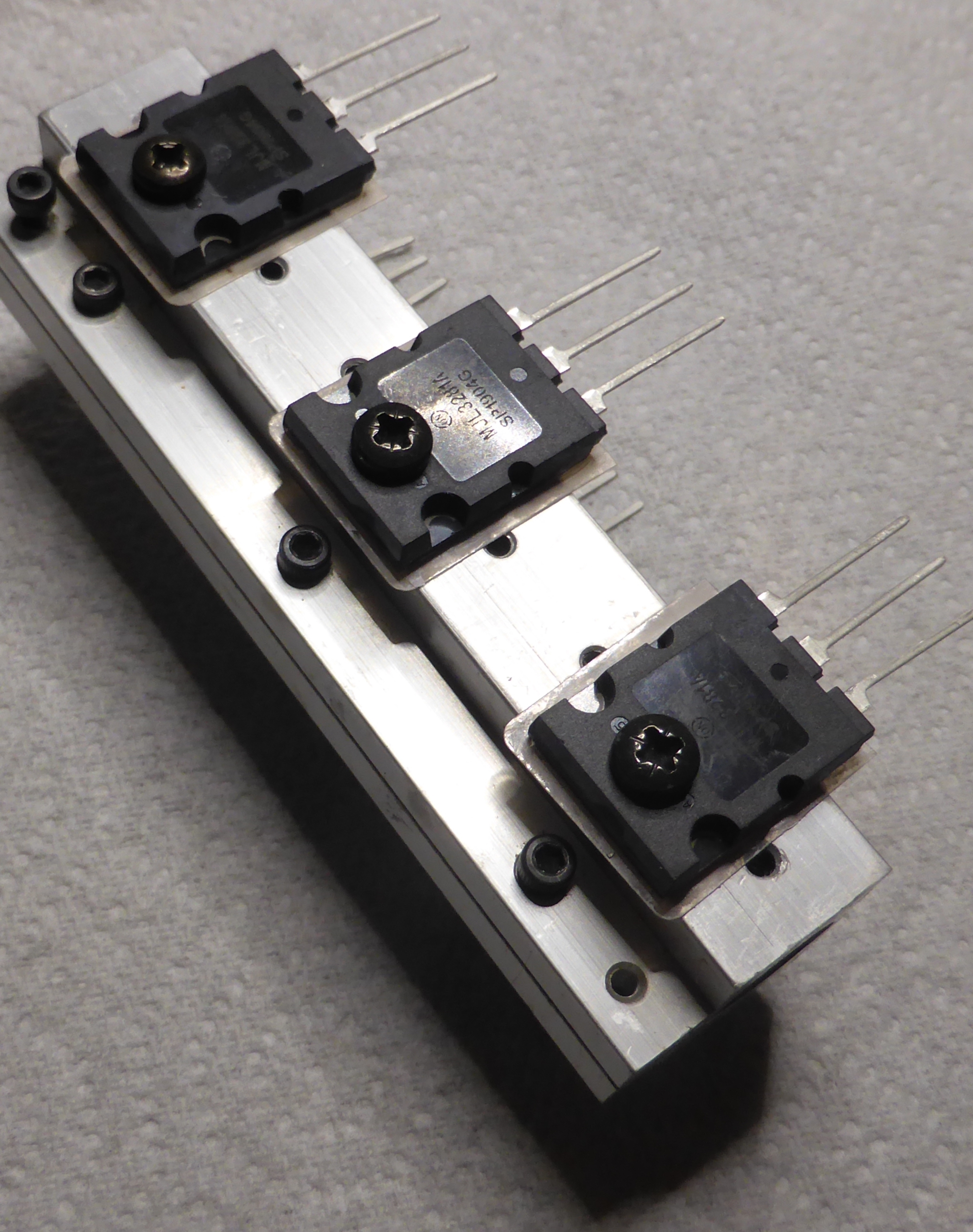
The new transistors fitted to the heatsink. This required drilling and tapping fixing holes, which should have been M3, but as you can see I have had a brainfart and done them M4 instead. Thinking it over, I like this better, it feels much more solid and secure. The insulators are 5 mil mica with a good overlap all round. |
|
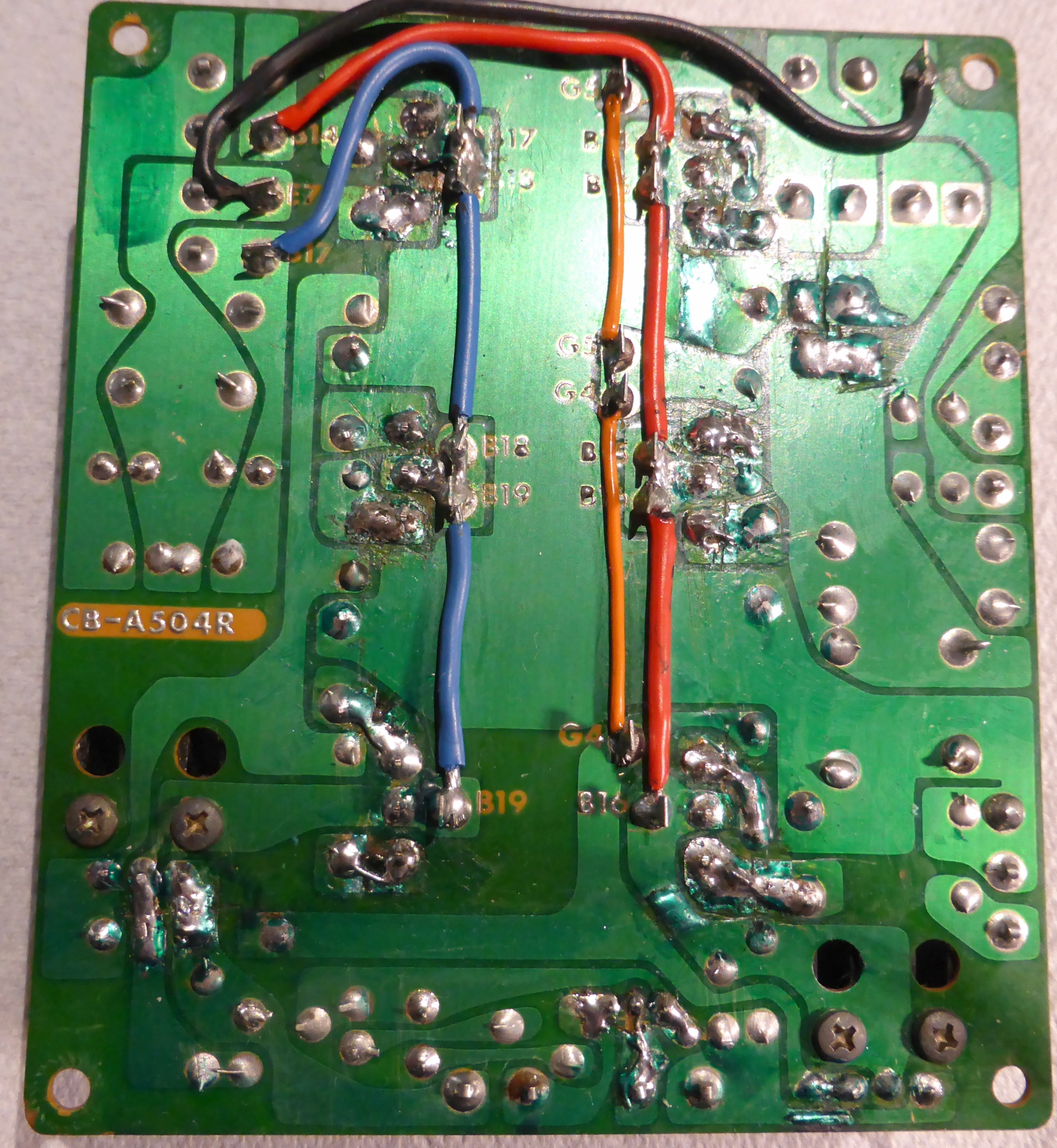
The underside of the repaired PCB. I have fixed the missing mask by just painting it on with a small brush. The wires I replaced because I didn't like the look of them. Not pretty, but better than it was. I think it was Sebastian de Ferranti who said "Ooh it's green! I like green!" |

|
The only damage to the right channel front end was failed pre-driver transistors and the series resistors.
subs: 2SC1904 --> MJE340 2SA899 --> MJE350 |
|
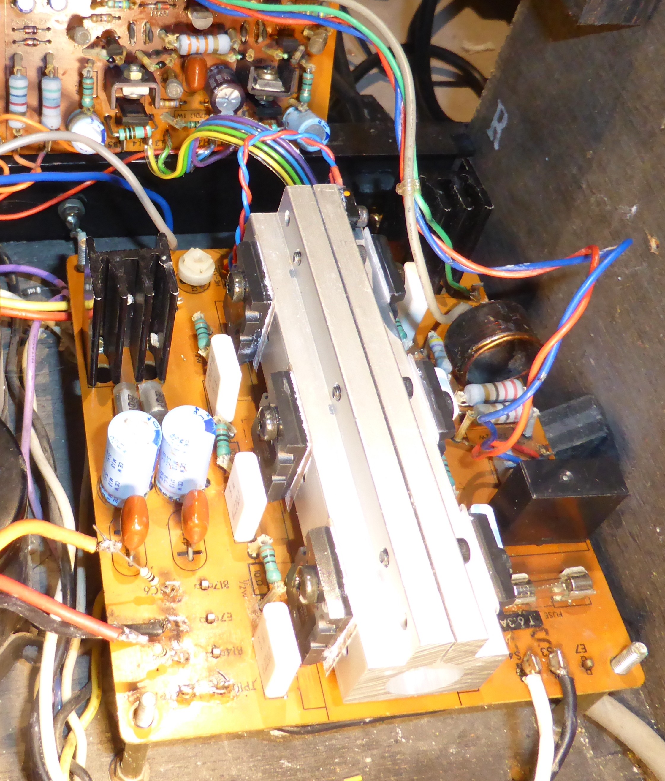
The repaired right channel PCB wired up for testing. I have left out the main heatsink to shorten the heating time.
2SC2565 --> MJL3281AG 2SA1095 --> MJL1302AG 2SC2238B --> MJE15032 2SA968B --> MJE15033 2SC2240 --> BC182L |
|
Now to take a look under the left channel, which is locked up hard with a saturated servo. Someone has replaced the transistors and emitter resistors but not bothered to clean the flux. But it's in much better shape than the right channel was. |
|
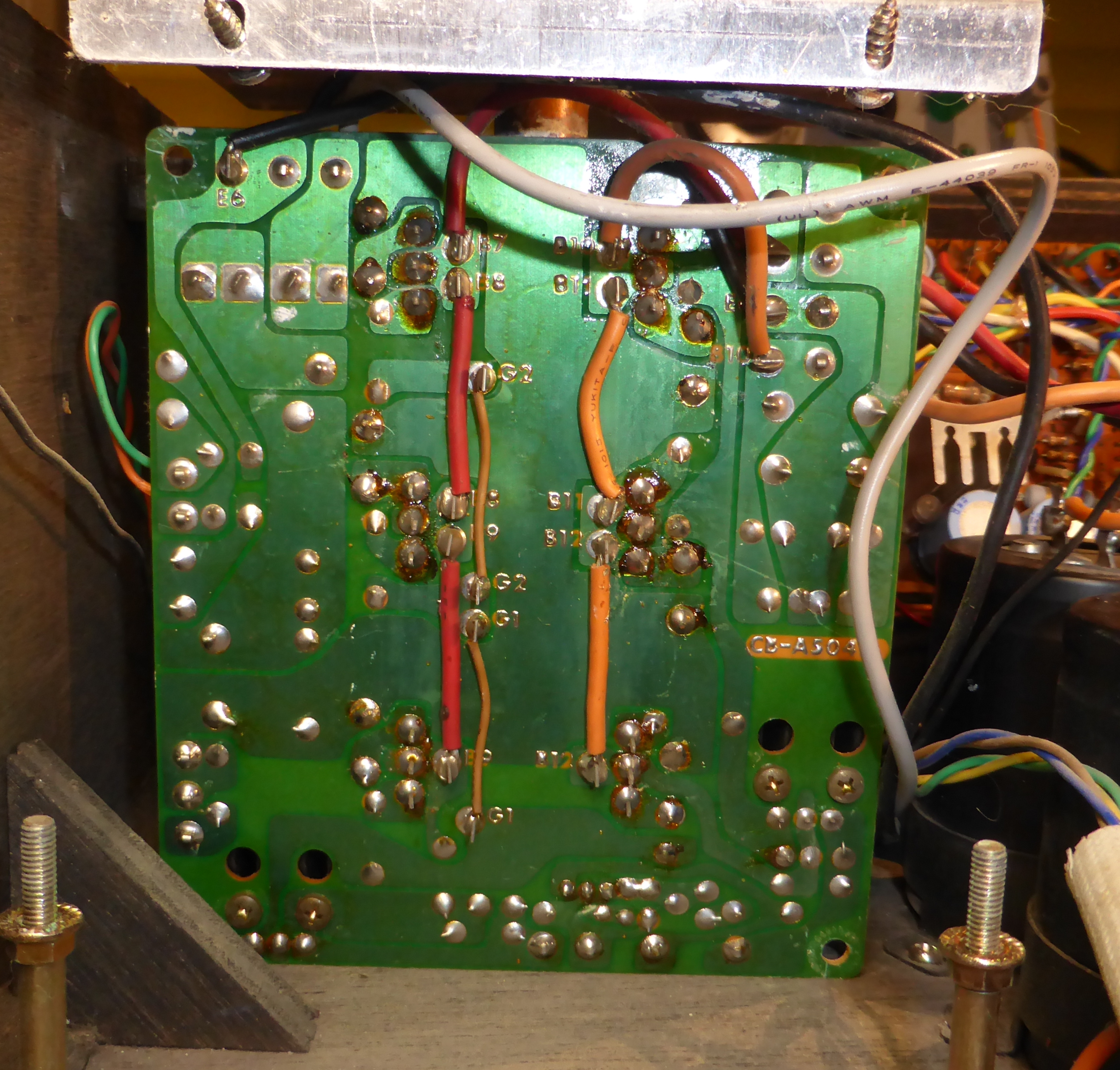
The left channel side of the back PCB shows signs that the pre-driver transistors have been replaced. This channel has obviously blown up at some time. |
|
The reason the left channel didn't work was because these two wires fell off. |
Other Stuff |
|
|
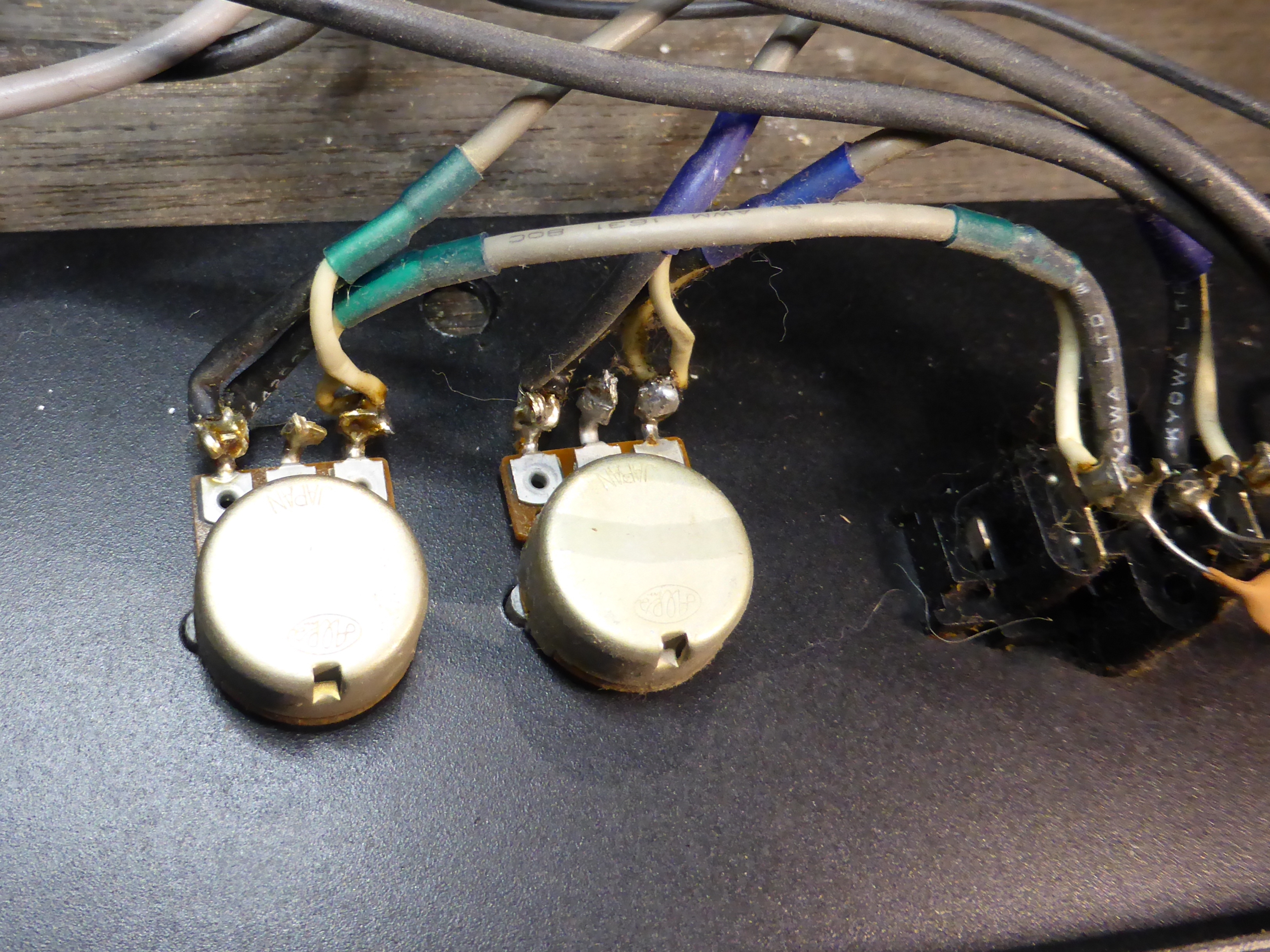
Someone has bypassed the input pots. |
|
A peculiarity of the design is that almost immediately after turn-off the output stage can sustain no quiescent current, so the big caps stay charged indefinitely. I have added a few bleed resistors. It still takes ages to discharge. |
|
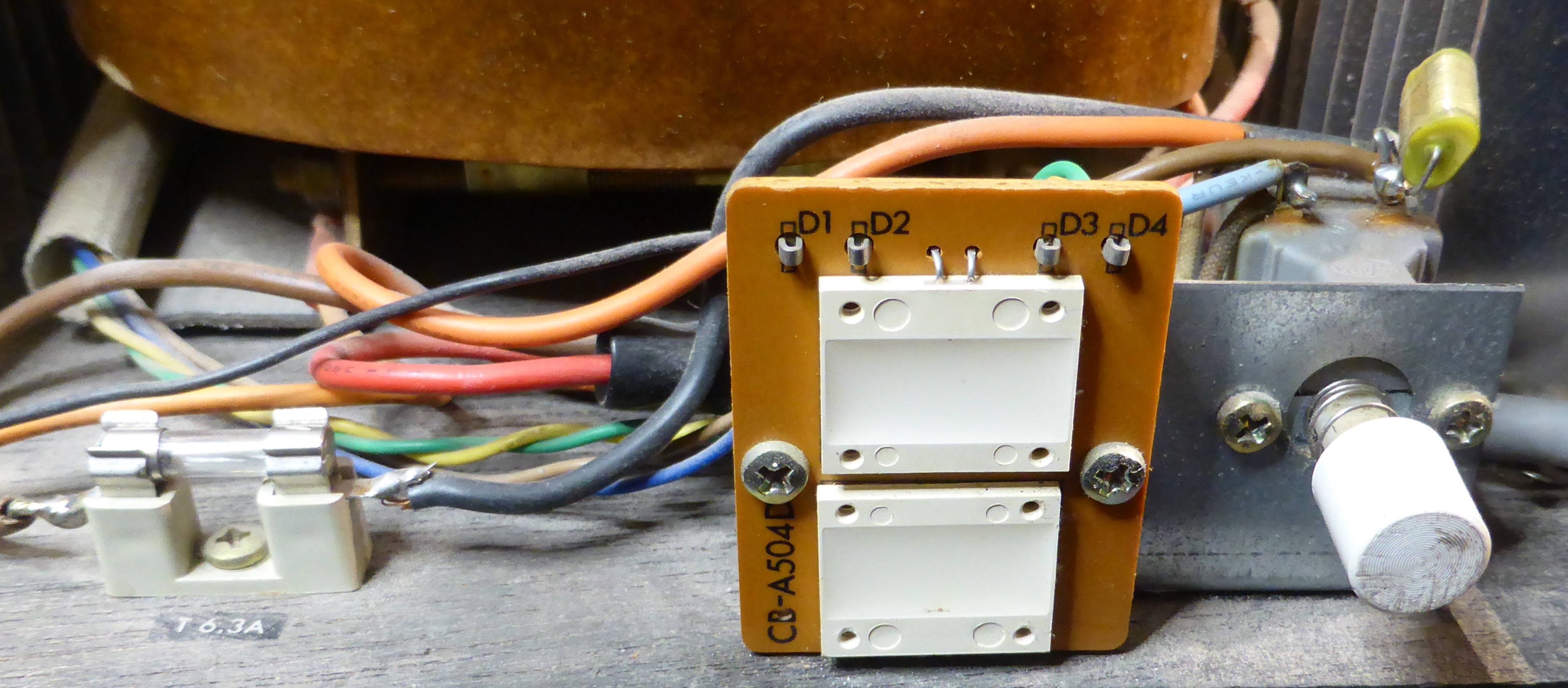
Power IEC on the back panel. Notice the lack of fuse. It is at the front of the amplifier near the switch. You have to remove the cover to check it. |
|
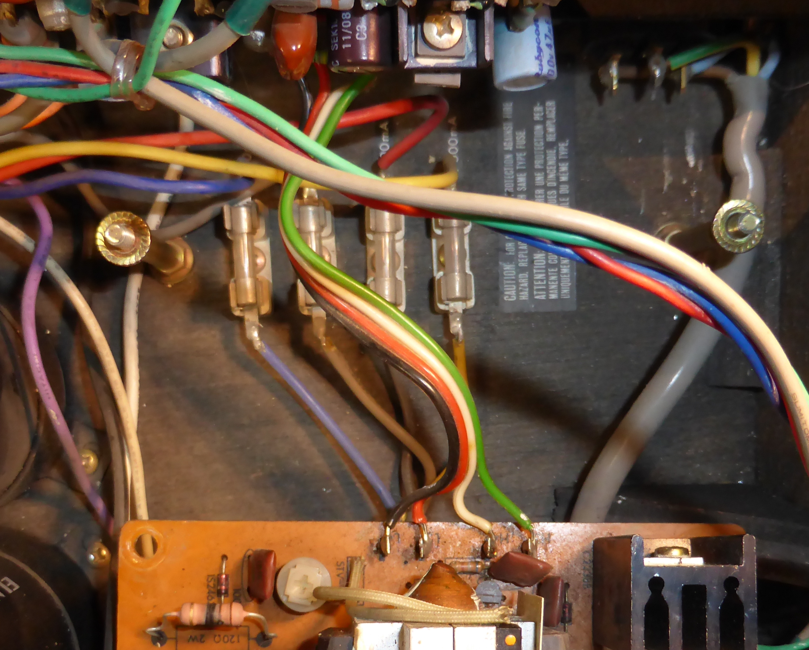
The rear PCB. Many of these wires were hanging by a thread and some came off while I was working on it. They are poor quality, but this is a sign that the PCB has been handled a lot. |
The Front End |
|
|
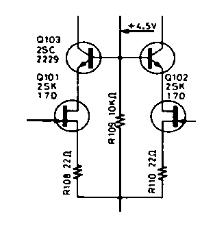
The current source for the input pair. An unusually high voltage from a 30V zener is placed over a 4k7 resistor, giving about 6mA for the pair. A little of this is taken to feed a divider which biases a cascode on the pair. |
|
The input stage is a slightly degenerated pair of FETs, cascoded at 5VDS. The BJTs are connected to a divider going from the current source to the rail. Looks like a bad idea but the rail is very stiff, so not a big deal.
|
|
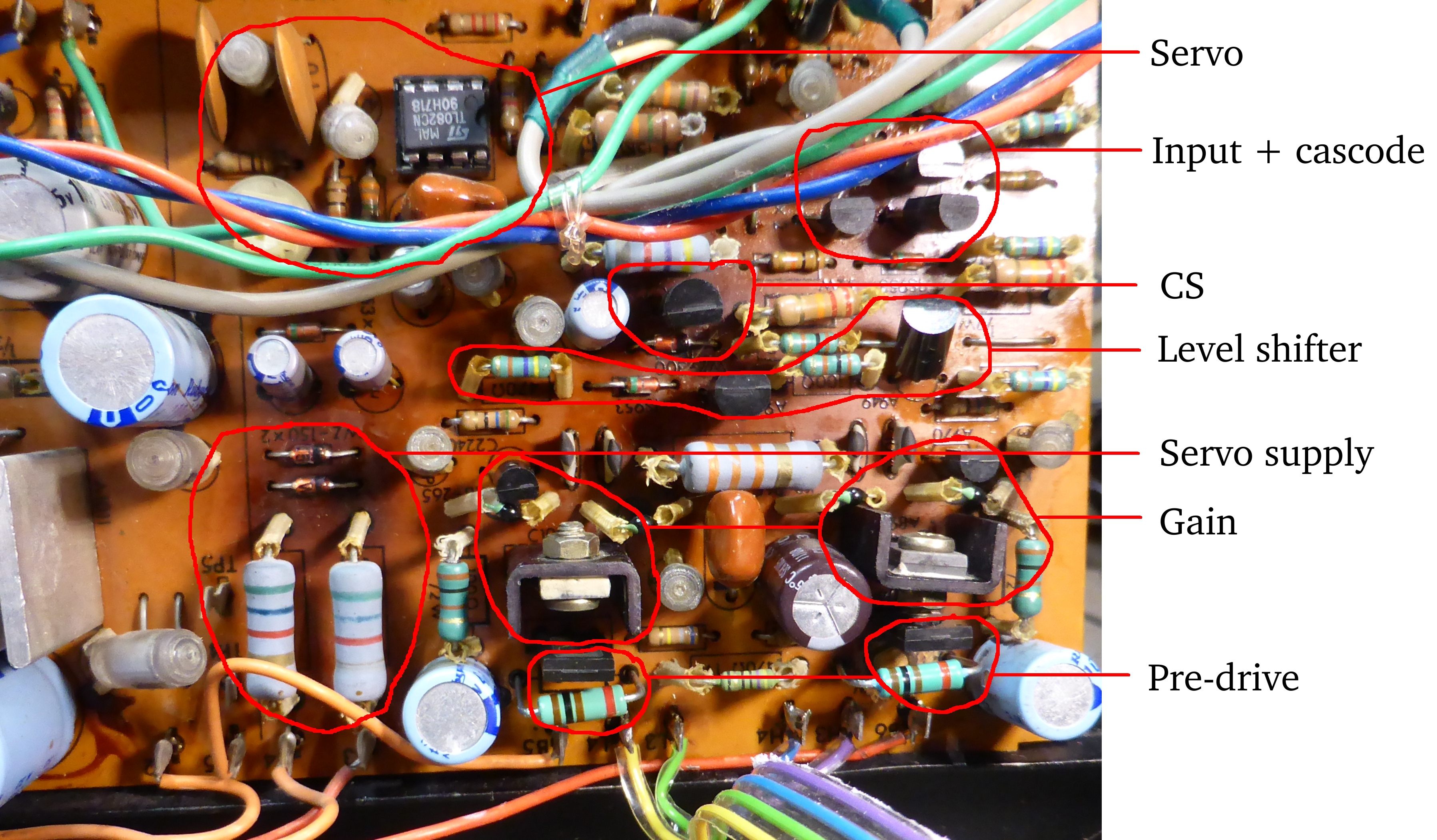
Layout of the right channel front end. The left is similarish. |
|
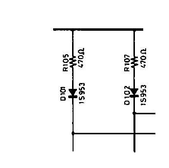
The input stage is not loaded by a current mirror, which you would normally expect, just a pair of 470 ohm resistors. Note how diodes are used here, I thought at first maybe to increase the drop for the next stage, but there is 1.5V which would be enough. Perhaps this is some sort of base-emitter junction compensation scheme. I've read about that sort of thing. But it does not feature in the grimoires of the Iichi, nor the Enchiridion Technologias of the Blessed Baxandall. |
|
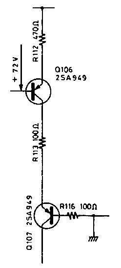
This is the level-shifter between the input stage and the lower voltage amplifier. There are two complementary opposing voltage amplifiers in this circuit, so this thing is needed to get appropriate drive to the lower one. Common-emitter feeds common-base, with component values selected for approximately unity gain. Note how the common-base has a 100 ohm resistor inserted in it. What the hell is that for? Extra distortion? Also there is another 100 ohm resistor between the two transistors, doing exactly nothing. It's insignificant compared to the impedance of the upper collector, and doesn't soak up any volts to take some stress off that transistor. This stage is the fugliest part of the works, which otherwise has a pleasing symmetry. |

|
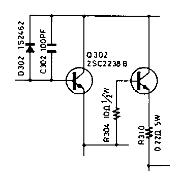
This is the upper of the two voltage amplifiers. Note how the amplifying device has its VCE pinned down to less than 2 volts by a bigger TO-126 transistor. My guess is the designer really wanted to use this particular 2SA970 transistor and its opposite number, which are a bit voltagely-challenged, so adopted this method to pin it as close as reasonably possible and save drive volts for the output tackle. The pass-through device no doubt has a high VCE rating, though I could find no info on it. It runs very hot, about 1W, and has a small heatsink. |

|
The last stage on the back panel, running from the regulated supplies is this pre-driver, using the same TO-126 devices as in the previous stage. Nice and clean and simple. Note how the 470 ohm resistor floats between the two emitters, rather than having two separate resistors to output, and this is repeated in the next driver stage. Very good practice and strange how so many amplifiers don't do that, even if only to save on resistors. |
The Output Stage |
|
|
The remainder of the amplifier is the fully-complementary output stage. Note the small diode from the driver base to rail. The front end runs from a regulated supply a few volts higher than the output stage, so it is possible an overdrive could happen. There is a 100 ohm resistor upstream which would limit current, but I don't like it, if it fails the whole output stage goes up in smoke. And I don't like the look of that small capacitor. It's also under a lot of unnecessary stress. Why not connect it to a ground rather than to the positive rail? Makes no sense, but I have seen the same thing on hundreds of amplifiers. |

|
My overall impression is that this is a very fragile amplifier, both physically and electronically. I imagine that there are very few of them in working order. Though the electronic design has some signs of competence, there are too many details to criticise. The lack of protection for the output transistors is worrying, also the direct-coupled input is looking for trouble.
|
end