RT-18 - Remodel of the Oktava MK-18 PCB

The RT-18 is a pcb which can be used to repair the Oktava MK-18
microphones. It is an improvement on the original PCBs, better
quality and with a solder mask on both sides and a partial ground plane.
It offers higher electrical insulation properties and greater resistance to humidity.


The pcb is designed so that it can be used to build a copy of the original circuit
using high quality modern components.


RT-18 pcb image
Price £7.50 with free p&p in UK.
£3.50 p&p for rest of world.
Redrawn schematic circuit diagram, click image for pdf, or right-click > view image to see png bitmap image.


Component notes


For the small capacitors, I have used a 200mil lead spacing which will suit many plastic film types and COG ceramics.


About the FET and BJT


There are two active devices. They are configured as a voltage follower.There is no reason not to use the original Russian FET if it is working well. It can be replaced with a very wide variety of devices because we have the luxury of two resistors in the drain to set up its operating point. I would recommend sticking fairly close to the original design current of 1mA. If it appears to be noisy or have a problem I would recommend something like a 2N3819 which have an IDSS of several milliamps.


If you reuse the original Russian FET, some of them have a fourth wire connected to the metal case, which can be snipped off close to the case. This will reduce the capacitance around the FET channel by a picofarad or two, and also reduce the chances of any creep, very tiny advantages but they cost nothing. As always with FETs, it is a good idea to clean between the legs with some alcohol and a small brush before you solder it into place.


The BJT in the mic I examined had no identication except for the letter E printed on the front. Nothing special about it other than the unusual BCE pinout.


I have designed the new PCB with centre-gate footprint for the JFET and ECB pinout for the BJT.
Some photos of an early MK-18, lent to me by Mr Chris Crane, who prompted me to design this PCB. I hope to get some photos from him of this mic with a new PCB installed.


To see full-size image, right-click > view image, then click on image.
Oktava MK-18 front view
Oktava MK-18 back view
Case opened showing how the switches work
The switch operating thingy and headbasket
The diaphragm is in good condition. This seems to be very heavy gold deposition compared to many modern capsules
The transformer connections do not correspond to the original Oktava diagram which is available various places on the interweb, the secondary centre-tap is used to feed the electronics directly rather than through the two resistors shown on the outer terminals. The switch connections are also incorrect on that diagram
The FET and BJT. The orange thing which looks like a capacitor is the BJT
Back case switch-operating tackle
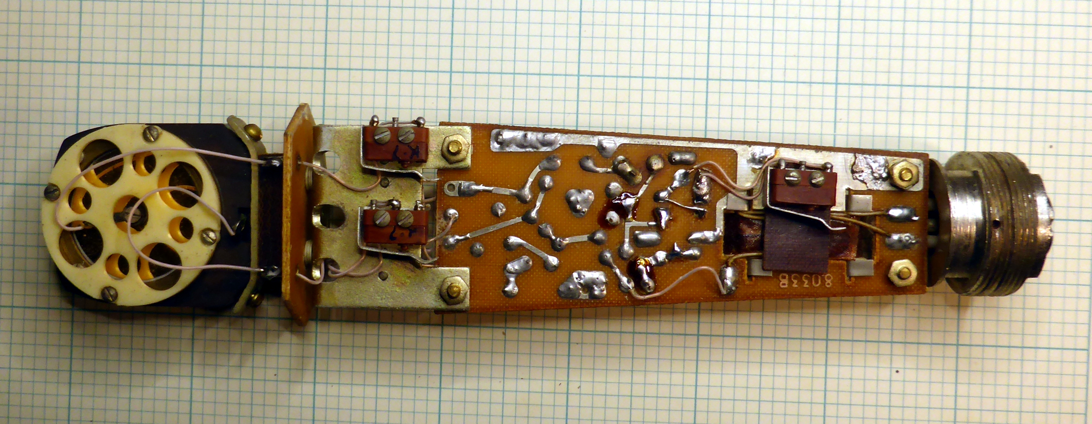
Top (front)
Solder side (back), switches 3, 4 and 5
Close-up of pattern selector switches 1 and 2
A complicated capsule mounting assembly. I think it would be better to not use the terminals and pass the wires straight through some holes in the board
Switches 3 and 4
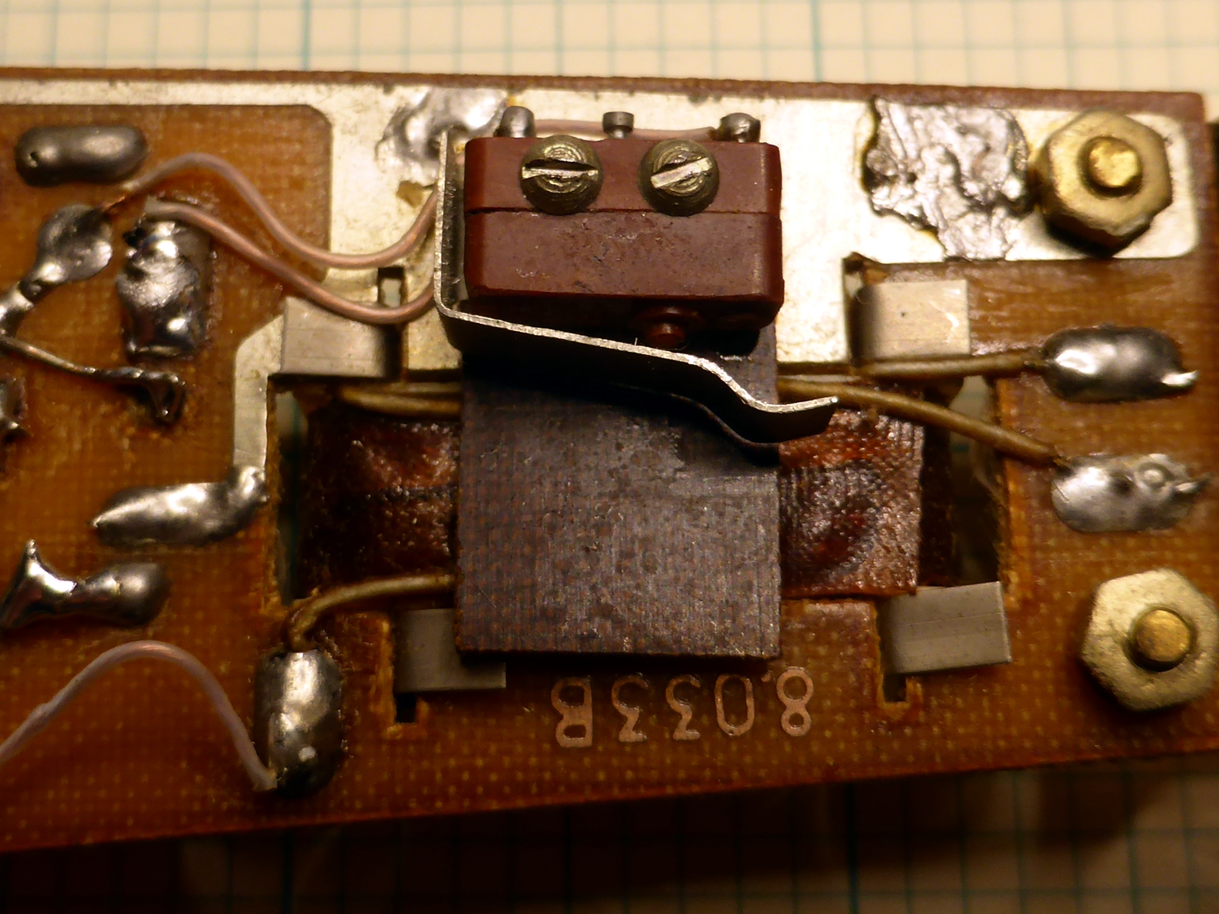
Switch 5 mounted under the transformer
Looks like someone made some small mistakes in the tracking which had to be bodged with pieces of wire. It's not easy designing PCBs without computer assistance. Been there, done that.
Note how the flanges at the connector end are on top of the PCB (ie component side), while at the capsule assembly end are on the bottom of the PCB. A spacer under switch 5 raises it to the same height as switches 3 and 4. Embiggen this picture for a better look.
end